CATEGORIES:
BiologyChemistryConstructionCultureEcologyEconomyElectronicsFinanceGeographyHistoryInformaticsLawMathematicsMechanicsMedicineOtherPedagogyPhilosophyPhysicsPolicyPsychologySociologySportTourism
Devices programmed
PLDs are used for storing logic functions. The categories in Fig. 3.1 show that there are three variants: PLAs, PALs and. LCAs. The differences between them are in respect of programming flexibility. PALs (programmable array logic) are the easiest to program. They are therefore particularly popular and are available in a wide range of designs. PLAs (programmable logic arrays) are basically more flexible, but programming them is more complicated. They have therefore ceased to be of major importance. LCAs (logic cell arrays) are very recent components. They can not only be programmed as various individual PLDs, but also with any data paths between those PLDs. This enables them to replace simple gate arrays. They can therefore also be described as user-programmable gate arrays.
When logic functions are implemented using the standard product terms, it is first necessary to AND together the input variables and then form the sum of the products. In order to be able to show these operations clearly, we use the simplified representation in Fig. 3.38. The internal design of PLAs and PALs can then be illustrated very easily, as shown in Fig. 3.39. The input variables of their negation and the intersecting inputs of AND gates form a matrix which enables all the required logical products to be formed. In a corresponding second matrix, the connections between the AND gates and the OR gates can then be established in order to form the required logical sums. This requires only one OR gate per output variable. In the case of a PLA (Fig. 3.39a), both matrices arc user-programmable. In the case of a PAL (Fig. 3.39b), the OR matrix is permanently preset (fixed) by the manufacturer, and only the AND matrix can be programmed.
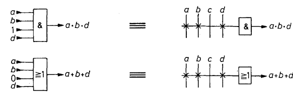
Fig. 3.38 - Simplified representation of the AND and OR operations. The crosses indicate which input is connected. An unconnected input has no effect since it is 1 for the AND operation and 0 for the OR operation.
A PROM can also be understood as a function memory if the address decoder, having a truth table as shown in the left half of Fig. 3.40, is interpreted as an AND matrix. Then we can make use of the representation in Fig. 3.39. For every address applied, only a single AND operation is 1, namely that corresponding to the address applied. There are therefore n = 2N product terms, whereas the PLAs and PALs have substantially fewer. Whether the associated function value is 1 or 0 is determined by the programming of the OR matrix.
PROMs designed for implementing logic functions are also known as PLEs (programmable logic elements). The differences become apparent by considering the example in Fig. 3.40. All the connections not required for these functions have been programmed "open". Figure 3.41 shows that all the required logical products are formed in the AND matrices of the PLA and PAL. In the case of the PLA, it is even possible to use a product, which is required several times, twice in the OR matrix. This freedom is not available in the case of the (simple) PALs, as their OR matrix is not programmable.
With a PROM, it is always the particular product corresponding to the input combination that is 1. Consequently, it is necessary in the OR matrix to program connections for all combinations that are 1 in the truth table. We can see from this that a PROM is the image of the truth table, whereas the PLA and PAL represent the logic functions. A PROM can be used to store any kind of truth table, whereas only a limited number of products and sums are available in a PLA or PAL. For this reason, it is not possible to realize any truth table, but only those which can be convewrted into simple logic functions. This requires utmost simplification of the functions using Boolean algebra and, if necessary, transformation from AND into OR operations using De Morgan's Law, in order to utilize the PALs as efficiently as possible. Nowadays this is no longer done manually but using special design programs which can be run on any personal computer. Their application is described in greater detail in Section 3.42.
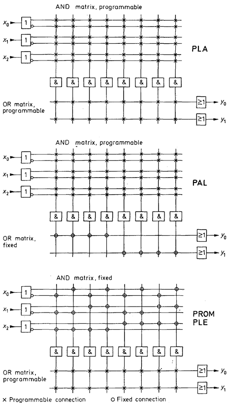
Fig. 3.3 9 - Comparison of the structures of PLA, PAL and PROM/PLE devices.
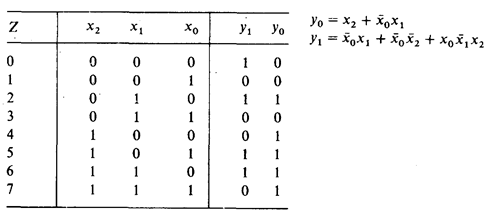
Fig. 3.40 - Example of a truth table and its logic functions.
Programmable logic array (PAL)
PALs are the principal representatives of programmable logic devices (PLDs). They are available in a wide range of variants, all of which are based on the principle shown in Fig. 3.39b. The differences are in the implementation of the OR operations at the output. The most commonly used variants are listed in Fig. 3.42. Each different type is designated by the relevant letter shown.
The high (H) output represents the basic type shown in Fig. 3.39. In the case of the low (L) type, the output is negated. The C output is complementary. In the programmable (P) type, the user can define whether the output function or its inversion is true. For this purpose the exclusive-OR output gate is used, whose second input can be made 0 or 1 by the programming. The user has then the freedom to form the negated function and thereby utilize the PAL more efficiently if necessary. In the case of the EXOR (X) output, there is likewise an exclusive-OR gate at the output; however, it is controlled by two OR operations. This variant is used for simple implementation of adders.
The sharing (S) output has features in common with the PLAs. Here the OR matrix is also partly programmable: two adjacent OR gates can share the AND operations available to them. This makes it possible to form functions for which the number of OR gates would otherwise be insufficient.
With many PALs, an output can also be used as an input or programmed as a bidirectional port (I/O). This is the purpose of the tristate gate at the output, whose ENABLE is itself a logic function.
An important application of PALs is in sequential logic systems. In order to obviate the need for additional chips, the required registers (R) are incorporated in the PALs. They have a common clock terminal to enable construction of synchronous systems. In addition, the output signals are generally fed back internally to the AND matrix, thereby eliminating external feedback circuitry and saving on pins.
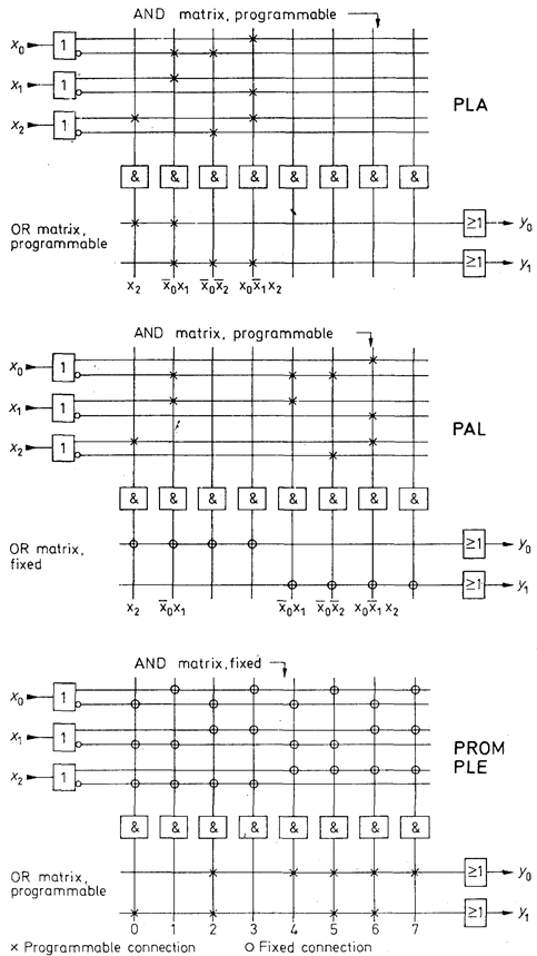
Fig. 3.41 - Implementation of the functions of Fig. 3.40 using a PLA, PAL and PROM.

Fig.3.42 - Output circuit of PAL.
PALs are also available which are designed for implementing asynchronous sequential logic systems. They allow the clock for each register to be defined by an additional logic function (AR in Fig. 3.42). In addition, these PALs usually have a freely definable set and reset function. Similar to the synchronous type, they may have internal feedback features.
Using the optimum PAL for each application would require a large number of different types - as Fig. 3.42 shows. In order to reduce the variety of types, PALs with a programmable output structure are becoming increasingly common. One such variable "macrocell" (V) is also shown in Fig. 3.42. It is built around a multiplexer which can be used to select any of four different operating modes. These are defined by programming the function bits f0 and f1. The different operating modes are listed in Fig. 3.43. Bit f0 determines whether or not the output is negated. Bit f1 switches between combinatorial and registered mode. It also determines, via a second multiplexer, whether feedback is taken from the output or from the register. We can see that most PALs can be implemented in this way using a single type.
| f1 | f0 | Type | Output | Feedback |
| H | Function | Output | ||
| L | Function, negated | Output | ||
| R | Register | Register | ||
| R | Register, negated | Register |
Fig. 3.43 - Operating modes of the variable macrocell.
Date: 2015-01-12; view: 1751
| <== previous page | | | next page ==> |
| Dynamic RAM controllers | | | National Security is put at risk with counterfeit electronic components in military and defence equipment poses a national security risk. |