CATEGORIES:
BiologyChemistryConstructionCultureEcologyEconomyElectronicsFinanceGeographyHistoryInformaticsLawMathematicsMechanicsMedicineOtherPedagogyPhilosophyPhysicsPolicyPsychologySociologySportTourism
Dynamic RAM controllers
To operate dynamic RAMs, additional circuitry is required. For a normal memory access, the address has to be loaded into the RAM in two consecutive steps. To avoid loss of data it is necessary to call up all the row addresses at least once within (usually) 8 ms. If the contents of memory are not read out cyclically, extra circuitry is required to effect cyclic addressing between normal memory accesses. These circuits are referred to as "dynamic RAM controllers". Figure 3.36 shows the block diagram for a circuit of this type [3.2, 3.3].

Fig. 3.36 - Design of a dynamic RAM controller for 1 Mbit RAMs.
AC = Address Strobe
RAS = Row Address Strobe
MA = Memory Address
CAS = Column Address Strobe
For a normal memory access, the externally-applied address is stored in the row and column address latch when address strobe AS becomes 1, indicating that the address is valid. An access cycle is simultaneously initiated in the timing and control block, and first, row address d0 ... a9 is forwarded to the memory via the multiplexer. Then, the row address strobe becomes 1, causing the address to be transferred to memory. Subsequently the column address a10 … a19 is produced and also read into memory with the column address strobe. This sequence is illustrated in Fig. 3.37. Following address input, the address strobe has to remain at logic 1 until data transmission is completed. The next memory access may not occur immediately, but only after a "precharge time" which is of the same order of magnitude as the address access time.
In order to perform the refresh, the lowest 512 addresses must be applied once every 8 ms. For a refresh cycle time of 300 ns, a total of some 150 ms is required for this purpose. Memory availability is thereby reduced by less than 2%. Three different methods can be used to organize the refresh time:
1) Burst refresh. In this mode, normal operation is interrupted after 8 ms and a refresh is performed for all memory cells. In many cases, however, it is undesirable for the memory to be inaccessible for 150 ms.
2) Cycle stealing. To avoid disabling the memory for a continuous 150 ms period, the refresh process can be subdivided and spread out over 8 ms: if the status of the refresh counter is incremented by one every 15 ms, then after 512 • 15 ms » 8 ms all the row addresses will have been applied once, as required. With cycle stealing the processor is stopped every 15 ms for one cycle and refresh step is performed. For this purpose, the refresh time base shown in the block diagram in Fig. 3.36 reduces the frequency of the clock signal CLK so that the timing and control block receives a refresh command every 15 ms.
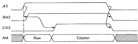
Fig. 3.37- Address input timing sequence for a dynamic RAM.
When a refresh cycle is initiated, the status of the refresh counter is transferred via the multiplexer to the memory and the RAS signal is temporarily set to 1. The counter is then incremented by 1. During the refresh cycle, the memory user is inhibited by a wait signal. This means that the on-going process is stopped very 15 ms for 0.3 ms, i.e. likewise slowed down by 2%.
3) Transparent or hidden refresh. With this method, a refresh step is also performed every 15 ms, but the refresh controller is synchronized in such a way that, instead of inhibiting the memory user, the refresh is performed at the precise instant when the user is not accessing the memory. This means that no me is lost. If any overlapping of an external access with the refresh cycle cannot be totally eliminated, an additional priority decoder (arbiter) can be employed, s shown in Fig. 3.36. It acknowledges an external request with a wait signal tttil the current refresh cycle is complete and then executes the request.
| Refresh controllers: | |||
| for 256k-RAMs: | THCT4502 | CMOS | Texas Instr., VTI |
| DP8420A | CMOS | National | |
| 74 F 764 | TTL | Signetics | |
| for 1M-RAMs: | SN74ACT4503 | CMOS | Texas Instr. |
| DP 8421 A | CMOS | National | |
| 74 F 1764 | TTL | Signetics | |
| TTL | AMD | ||
| for 4M-RAMs: | DP 8422 A | CMOS | National |
| Am 29 C 688 | CMOS | AMD |
Date: 2015-01-12; view: 1648
| <== previous page | | | next page ==> |
| Dynamic RAMs | | | Devices programmed |