CATEGORIES:
BiologyChemistryConstructionCultureEcologyEconomyElectronicsFinanceGeographyHistoryInformaticsLawMathematicsMechanicsMedicineOtherPedagogyPhilosophyPhysicsPolicyPsychologySociologySportTourism
ROM with singl programming
Read-only memories (ROMs)
The term ROM refers to table memories which are normally only read. They are therefore suitable for storing tables and programs. Their advantage is that the memory content is retained when the supply voltage is disconnected. Their disadvantage is that putting data into the table is much more intricate than with RAMs. The categories shown in Fig. 3.1 (MROM, PROM, EPROM, EEPROM) differ with respect to the input procedure.
Mask-programmed ROMs (MROMs)
With these devices, the memory content is entered during the final manufacturing stage using a specific metallization mask. This process is only cost-effective for large production quantities (from 10,000 approx.) and generally requires several months for implementation.
Programmable ROMs (PROMs)
A PROM is a read-only memory whose content is programmed-in by the user. The programmable components are usually fuses which are implemented in the ICs by means of exceptionally thin metallization links. Diodes are also used, which can be shorted by overloading them in the reverse-bias direction. The latest programmable elements for PROMs are special MOSFETs with an additional "floating gate". This is charged up during programming, causing it to change the pinch-off voltage of the MOSFET. As the floating gate has all-round SiO2 insulation, it can be guaranteed to retain its charge for 10 years.
We shall now describe the internal design of a PROM using the example of the fuse-type PROM in Fig. 3.21. For technological reasons, the individual memory cells are not arranged linearly but as a square matrix. A particular memory cell is addressed by applying a logical 1 to the appropriate column or row connection. For this purpose the address vector A = (a0 ... an) must be decoded accordingly. The column and row decoders used operate as 1-out-of-n decoders.
The memory cell selected is activated by the AND gate at the intersection of the selected row or column line. The ORing of all the memory cell outputs produces output signal D. In order to obviate the need for a gate with 2n outputs, wired-OR logic is used. In the case of open-collector outputs, this can be implemented by wired-ANDing the negated signals.
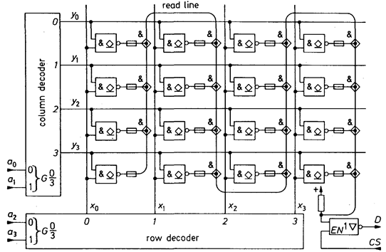
Fig.3.21 - Internal structure of a PROM. Example showing 16-bit memory capacity.
In its basic state, each memory cell addressed generates output signal D = 1. To program a zero, the fusible link at the output of the desired cell is blown as follows. One selects the address of the corresponding cell, turning on the output transistor of the NAND gate. A powerful current pulse is then injected into the read line which is just large enough to blow the fusible link at the NAND gate output. A timing sequence precisely denned by the manufacturer must be adhered to. Special programming devices are therefore used, which can be tailored to the particular type of memory.
In the case of PROMs, not just 1 bit but an entire 4-bit or 8-bit word is usually stored at an address. These devices therefore possess a corresponding number of data outputs. Specifying a memory capacity as, say, 1 k x 8 bits means that the memory contains 1024 8-bit words. The contents are specified in the form of a programming table. By way of example, Fig. 3.22 shows its organization for a 32 x 8-bit PROM.
The circuit symbol of a PROM is like that of the RAM in Fig. 3.5. The write-read switch here becomes the programming input and the data inputs are omitted.
Figure 3.23 lists some of the more common PROM types realized in various technologies.
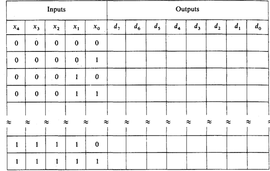
Fig. 3.22 - Example of a programming table for a PROM containing 32 8-bit words.
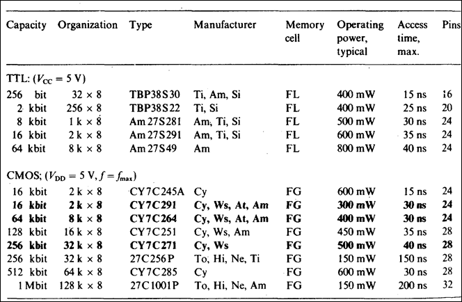
Fig. 3.23 - Examples of PROMs.
Manufacturers: Am = AMD, At = Atmel, Cy = Cypress, Hi = Hitachi, Ne = NEC,
Si =Signetics, Ti = Texas Instr.
Memory cell: FL = fusible link, FG = floating gate = MOSFET
UV-erasabIe PROMs (EPROMs)
An EPROM (erasable PROM) is a PROM which can not only be user-programmed, but also erased with ultraviolet light. MOSFETs incorporating an additional floating gate are used exclusively as the memory element. This is charged up during programming (as with many PROMs), thereby changing the pinch-off voltage of the transistor. With EPROMs, however, this charge can be erased again in about 20 minutes by irradiation with UV light. For this purpose, I the package is provided with a quartz glass window. Due to the additional package complexity involved, EPROMs are more expensive than non-window PROMs, even though they are realized in the same technology. Consequently, EPROMs are useful at the development stage of equipment, but for equipment mass production, the equivalent PROMs are to be preferred.
EPROMs are programmed on a word-by-word basis, i.e. for the usual 8-bit I organization one byte at a time. In the case of older EPROMs (e.g. 2716; 2 k x 8 bit) the programming procedure is still simple. One applies a programming voltage of VPP = 25 V, together with the required address and the bit I pattern to be programmed. Then a programming command lasting 50 ms is applied to store the data. Programming can then be terminated or the process can be repeated for another address using the associated bit pattern. In the case of a 2-kbyte EPROM, programming the entire device takes about two minutes. However, programming a 128 kbyte memory would take almost 2 hours. As this is clearly not tolerable, it was necessary to modify the technology and programming algorithms for larger EPROMs. All fast programming algorithms are based on the fact that most of the bytes of an EPROM can be programmed in considerably less than 50 ms. However, as "slower" bytes occur from time to time, it is impossible to generally reduce the programming time. Instead, a variable programming pulse length is employed.
The "fast" or "intelligent" programming algorithm generally used nowadays is shown in Fig. 3.24. The programming voltage VPP = 12.5 V is applied and the supply voltage is raised to VCC = 6 V. The higher supply voltage speeds up the programming process, as the transistors assume lower impedance, and also constitutes the worst-case condition for verification purposes. The address then becomes A = 0 and the associated data are applied. Now follows the procedure for programming this byte. For this purpose, an auxiliary counter is set to n = 0. A 1 ms programming command is then issued. After the auxiliary counter has been incremented, the memory content is read out to check whether programming has already been successful. If not, up to another 24 programming commands are issued. If the byte has still not been programmed, the chip is deemed to be defective. Only a few programming pulses are normally required. However, it is still not certain that the floating gate has sufficient charge to last for 10 years. In order to make sure, the charge is trebled. This is done by overprogramming for 3n • 1 ms.
The first byte is thus programmed and the process can be repeated for the next address using new data. At the end of programming, we switch back to the read mode and check once more that the entire memory content is in order. The fast programming algorithm reduces the programming time for a 1 Mbit EPROM from around 2 h to less than 10 min. By reducing the programming pulse duration to 100 ms, times of less than 1 min can be achieved with some EPROMs.
Commonly used EPROMs are listed in Fig. 3.25.
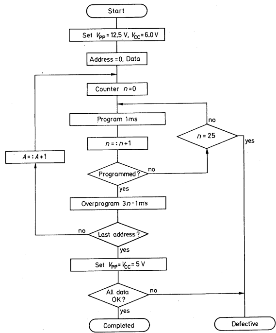
Fig. 3.24 - Fast algorithm for programming EPROMs.
| Capacity | Organization | Type | Manufacturer | Operating power, typical | Access time, max | Pins | |
| CMOS: (VDD = 5V, f = fmax) | |||||||
| 16 kbit | 2k x 8 | Cy7C291 | Cy, Ws | 250 mW | 35ns | ||
| 64 kbit | 8k x 8 | 27C64 | Ti, Fu, Na, Am | 100 mW | 150ns | ||
| 8k x 8 | 27HC64 | At, Cy. Ws | 300 mW | 45ns | |||
| 4k x 16 | WS57C65 | Ws | 300 mW | 55ns | |||
| 128 kbit | 16k x 8 | 27C128 | Ti, Fu, Am | 150 mW | 150ns | ||
| 16k x 8 | Cy7C251 | Cy, Ws | 400 mW | 45ns | |||
| 256 kbit | 32k x 8 | 27C256 | Ti, At, Fu, Hi, Mi, Ne, Na | 150 mW | 150ns | ||
| 32k x 8 | 27HC256 | At, Cy, Ws | 350 mW | 55ns | |||
| 16k x 16 | 27C202 | In, Ws | 500 mW | 55ns | |||
| 512 kbit | 64k x 8 | 27C512 | Ti, At, Fu, Mi, Ne, Na | 150 mW | 150ns | ||
| 64k x 8 | 27C285 | Cy | 700 mW | 30ns | |||
| 1 Mbit | 128k x 8 | 27C010 | Am, To, Fu, Hi, Mi, Na, In | 150 mW | 200ns | ||
| 64k x 16 | 27C1024 | Am, To, Fu, Ti, Mi, At, Na | 250 mW | 200ns | |||
| 64k x 16 | 27HC1024 | At, In | 500 mW | 55ns | |||
| 2 Mbit | 256 k x 8 | 27C2001 | Ne, In, Am | 200 mW | 200ns | ||
| 128k x 16 | 27C220 | In, Am | 250 mW | 200ns | |||
| 4 Mbit | 512 k x 8 | 27C4001 | Ne, Ws, To | 150mW | 150ns | ||
| 256 k x 16 | 27C240 | In, Hi, Am | 250 mW | 200ns | |||
Fig. 3.25 - Examples of EPROMs.
Manufacturers: Am = AMD, At = Atmel, Cy = Cypress, Fu = Fujitsu, Hi == Hitachi,
In = Intel, Mi = Mitsubishi, Na = National, Ne = NEC, Ti = Texas Instr., To = Toshiba, Ws = Wafer Scale
Date: 2015-01-12; view: 2043
| <== previous page | | | next page ==> |
| Hamming code | | | Memori element with electrical erase |