CATEGORIES:
BiologyChemistryConstructionCultureEcologyEconomyElectronicsFinanceGeographyHistoryInformaticsLawMathematicsMechanicsMedicineOtherPedagogyPhilosophyPhysicsPolicyPsychologySociologySportTourism
CHANNEL MOBILITY AND STRAIN
Starting with the 90-nm generation of MOSFETs, straining of the Si channel has been employed to improve the mobility of both electrons and holes. The strain affects the band structure, and successful strain engineering exploits this to reduce the effective mass in the desired direction of conduction. The strain is produced by stressing the channel region in a variety of ways, as we shall reveal. Hooke’s Law relates the deformation u of a 1-D object to the applied force F by a material-related force constant K :  When generalized to a 3-D object, such as a cube of crystalline semiconductor, we have normal forces and shear forces, and a proliferation of subscripts because of the possibility of deformations of a given side length in a given face arising from all the possible normal- and shear-forces. Each force per unit area is a stress and each component of deformation is a strain. The force required to produce a given strain is determined by the elastic stiffness constants of the material. In cubic crystals such as Si and GaAs, there are just three independent such constants. In Si, their magnitudes range from 64 to 166 GPa, which gives an indication of the immense pressures within a crystalline solid. Conversely, the strain that results from a given stress is determined by the elastic compliance constants of the material, which are related to the elastic stiffness constants. In the simple 1-D model that we used in Chapter 2 to illustrate how band structure is related to crystal structure, we saw the importance of the spacing between atoms. Thus, if this spacing is changed by strain, we can expect changes in band structure to result. If we are looking for strain to improve the mobility of holes in silicon, for example, it would be advantageous if the heavy-hole band could be lowered in energy with respect to the light-hole band.3 Unfortunately, it is not as simple as this in practice. Both valence bands become so warped by the strain that neither can be considered ‘heavy’ nor ‘light’. Instead, because the strain splits the bands, they are referred to as the ‘top’ and ‘bottom’ bands. As the holes preferentially occupy the higher band, it is important that the curvature of the top band be such that the effective mass in the desired direction of conduction be reduced. One way to achieve this for a <110> channel on a {001} Si surface in a sub-100 nm device is to apply a uniaxial compressive stress of about 1 GPa to the p-type channel. This is a huge pressure when one realizes that about 0.8 GPa will break high-strength steel! One way to realize such a high stress is to etch recesses in the Si where the source and drain should be, and then fill-in by epitaxially growing Si1−x Gex .With a Ge mole fraction of x ≈ 30 %, the more expansive SiGe puts the Si channel under a compressive stress of the required magnitude. To date (2009), hole mobility enhancements of up to about four times have been achieved by using this approach. For n-channel Si MOSFETs on {001} substrates, a <110> tensile stress induces a shear strain that is beneficial for electron conduction in this direction. Three notable changes in the conduction-band.structure occur: the six-fold symmetry of the conduction-band minima is broken, leading to the two [001] valleys moving to lower energies; the conduction-band minimum moves towards the X-point as the shear strain increases; the degeneracy of the two conduction-band minima at the X-point is removed. One manifestation of this is that the prolate spheroid constant-energy surfaces of become scalene spheroids, i.e., the two transverse effective masses are no longer equal. In other words, with reference to Fig. 1, the Brillouin zone is no longer symmetrical in directions perpendicular to the new kx-direction.
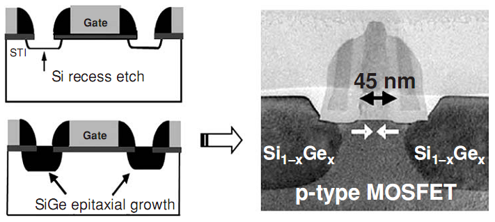
Figure 1. Partial process flow and TEM cross-sectional view of a strained-Si p-channel MOSFET using embedded SiGe for the source and drain regions
Partial process flow and TEM cross-sectional view of a strained-Si p-channel MOSFET using embedded SiGe for the source and drain regions. One manifestation of this is that the prolate spheroid constant-energy surfaces of become scalene spheroids, i.e., the two transverse effective masses are no longer equal. In other words, with reference to the Brillouin zone is no longer symmetrical in directions perpendicular to the new kx-direction. The situation is obviously quite complicated, and is made more so by quantum confinement effects in the narrow inversion layer. Here, we’ll just illustrate the beneficial effect of breaking the six-fold symmetry of the conduction bands extant in unstrained bulk material.
The equivalent constant-energy surfaces in 3-D are shown in. The four spheroids in the horizontal plane are often called the ∆4 valleys, and the two in the perpendicular direction are called the ∆2 valleys.Here, we consider the silicon channel to be in the surface plane. The tensile strain breaks the six-fold degeneracy of these valleys, raising the energy of the ∆4 set, and lowering the energy of the ∆2 set, i.e., the bottom of the conduction band is raised for the ∆4 valleys and is lowered for the ∆2 valleys. For a given energy E with respect to the bottom of the conduction band in the ∆4 valleys, E − EC for the ∆2 valleys is increased, so the spheroids become larger. The electrons naturally seek the lower energy states, so population of the ∆2 valleys is favoured. If the in-plane effective mass in the ∆2 valleys remains at  , which we note from is considerably less than the longitudinal effective mass
  , then the electron mobility in the channel is increased. As mentioned above, the effective masses are changed by the strain, but to get an idea of the enhancement in μe that might be possible,
consider the conductivity effective mass in. Based on the equal probabilities of occupation of the six equivalent conduction bands, a value of  ,COND = 0.26m0 was estimated. If all the electrons could now locate in the ∆2 valleys, For N-FETs a tensile liner is used, and its adhesion to the source and drain allows its inherent tensile stress to stretch the channel. The contact area in the former regions is much greater than the channel area, so any strain relaxation that takes place occurs mainly outside of the channel. This means that this method of stressing works well if the channel is short, but it also means that it is not easily scalable. In fact, at the 45-nm node, the source and drain areas may be insufficient to ‘anchor’ the stress liners. An alternative stressor would then be needed. Creating a trench and filling it with a material that would be compressed by the surrounding silicon is one possibility under investigation at present. It is amazing that such large and different stresses can be applied to such tiny structures that are in such close proximity. The influence of the tensile stress in an N-FET on the compressive stress of a neighbouring P-FET, for example, is likely to become a necessary consideration in layout design, if, indeed, it is not already so.
Date: 2015-01-29; view: 4504
| <== previous page | | | next page ==> |
| THE ON-CURRENT | | | Module Answers |