CATEGORIES:
BiologyChemistryConstructionCultureEcologyEconomyElectronicsFinanceGeographyHistoryInformaticsLawMathematicsMechanicsMedicineOtherPedagogyPhilosophyPhysicsPolicyPsychologySociologySportTourism
Conversion of BCD to straight binary code
In many cases the BCD code can be generated directly in a simple way, e.g. using BCD counters. As will be discussed later, many arithmetic operations can also be performed in BCD code, but sometimes conversion to straight binary numbers is necessary. This can be achieved by a repeated division by 2. To begin with, the binary coded decimal number is divided by 2, and if it is an odd number, a remainder of 1 is obtained, i.e. the 20-bit has the value 1. The quotient is again divided by 2. If the remainder is 0, the 21-bit is 0, and if the remainder is 1, the 21-bit has the value 1. The more significant bits of the straight binary number are obtained accordingly.
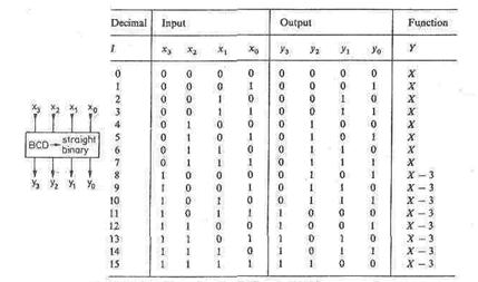 |
The division of a BCD number by 2 can be carried out simply by shifting it one place to the right, since the individual decades are already straight-binary coded. In each case, the remainder is the bit which has been "pushed out" of the BCD frame. If, during shifting, a 1 crosses the boundary between two columns, an error is incurred: when crossing from the tens to the units, the bit weighting of the shifted 1 must be halved from 10 to 5. However, for a straight binary number, the assigned weighting would be 8 so that, for a correction, 3 must be subtracted. Therefore the following correction rule applies: If the MSB of a column (decade) after shifting is 1, a subtraction of 3 is required in this particular decade. The truth table of the correction network in Fig. 1.52 can
Fig, 1.52 - Correction system for SCD-to-straight binary conversion.
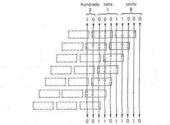
Fig. 1.53 - BCD-to-straight binary conversion by correction networks.
The values entered refer to the example of 218dec thus be directly determined. The conversion is complete when the BCD number has been entirely "pushed out" of the frame. Figure 1.53 shows a combinatorial logic system for the conversion of a 2  -digit BCD number. In analogy to Fig. 1.10 shifting of the BCD frame is achieved by hard-wiring identical correction networks. To illustrate the basic structure, all three correction networks required for each shift are shown. If the MSB is not used, no correction is necessary as can be seen in Fig. 1.52. and the correspondingcorrection networks can be omitted. In Fig. 1.53, they are shown by dashed lines.
The correction networks are available as blocks of five in the form of manufacturer-programmed 256-byte ROM (SN 74 S 484). To convert two BCD decades, one 1C is required. Four BCD decades require five ICs.
1.11 Shifters
A simple shifter, shown in Figure 1.54, is a combinational module that has an (n+2)-bit input x, an n-bit output y, and two 1-bit control inputs: d (for the direction of shift) and s (for shift or no-shift).
To construct networks of shifter modules, it is convenient to have the output controlled by an enable input E so that the output is 0 when E=0.
The output corresponds to the input x = (xn, xn-1, . . . ,x0, x-1) shifted one bit left, one bit right, or unchanged as specified by the d and s inputs. The shifter operation is specified as follows:
| yi= | xi-1 if d= 1 and s = 1 and E= 1 (left shift) |
| xi+1 if d=0 and s = 1 and E= 1 (right shift) | |
| xi if s=0 and E=1 (no shift) | |
| 0 if E=0 |
where 
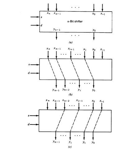
Fig. 1.54 - n-Bit simple shifter. (a) Block representation, (b) ”right shift” , (с) “ lefte shifter”.
The leftmost and rightmost values are specified by means of the variables x-1 and xn. In left shift y0 =x-1 and in right shift yn-1=xn. Some typical cases for the values of these additional variables are
| x-1= | 0 left shift with 0 insert |
| 1 left shift with 1 insert | |
| xn-1 left rotate |
| xn= | 0 right shift with 0 insert |
| 1 right shift with 1 insert | |
| x0 right rotate |
A simple shifter can be implemented with gates, multiplexers, or pass-transistors as shown in Figure1.55.
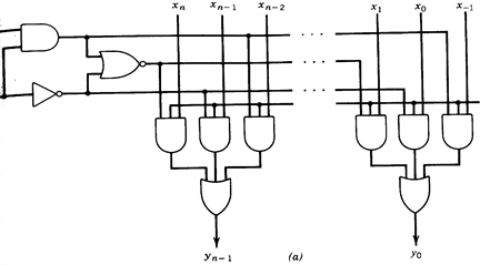
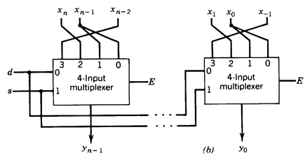
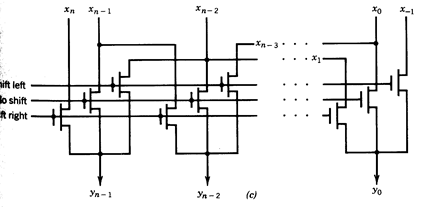
Fig. 1.55 - Simple-shifter implementation (a) with gates, (b) with multiplexer and (c) with pass transistor.
A p-shifter is a generalization of the simple shifter in which the amount of shift can be 0,1 , . . . , p to the left or to the right (bidirectional p-shifter). The shift distance is specified by a control vector s of [log2(p+ l)] bits and the shift direction by the input d. The input vector has n+2p bits. The subvectors (  , . . . , xn) and (x-1, . . . , x-p) provide the additional bits required for the shifts (Figure 1.56.a).
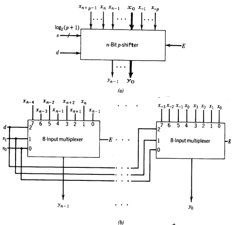
Fig. 1.56 - n-Bit p-shifter. (a) Block diagram, (b) n-bit 3-shifter implementation.
A high-level description of the p-shifter module is
| yi= | xi-s if d=1and E=1 (left shift) |
| xi+s if d=0 and E=1(right shift) | |
| 0 if E=0 |
where s is the shift distance and 0 £ i £ n-1.
An implementation of a 3-shifter using multiplexers is shown in Figure 1.56.b.
Date: 2015-01-12; view: 5326
| <== previous page | | | next page ==> |
| Code converters | | | Shifter Networks |