CATEGORIES:
BiologyChemistryConstructionCultureEcologyEconomyElectronicsFinanceGeographyHistoryInformaticsLawMathematicsMechanicsMedicineOtherPedagogyPhilosophyPhysicsPolicyPsychologySociologySportTourism
Levels of Integration
TL chips contain a range of number of gates. According to this number have SSI, MSI, and LSI chips.
SSI chips contain several independent gates, with inputs and outputs going to pins in the package. The number of gates is limited by the number of pins in the package, typically 14 to 16 pins.
MSI chips contain up to 100 gates and implement functions such as decoders, multiplexers, registers, counters, and adders. The number of gates is again limited by the number of pins, since these functions still have a relatively low gates per pin ratios.
LSI chips contain up to 500 gates. They implement functions such as bit-slice processor elements, memory, and I/O controllers. The number of gates that can be included in a chip is limited by the area (occupied by the gates and the connections) and by the power dissipation.
Other bipolar technologies, I/O compatible with TTL, implement VLSI chips with up to 2500 gates per chip. They include building blocks that are used in the implementation of microprogrammed and computers and controllers.
On-Chip and Off-Chip Connections
In the implementation of the MSI/LSI chips it is possible to distinguish two types of gates: those that are totally internal to the chip, having no direct connection to the pins of the chip, and those that are connected to the external pins, especially to the output pins. The first type of gate can be low-power and does not require totem-pole outputs since its load is internal and is characterized by a small capacitance. On the other hand, the gates that drive the external output might require a totem-pole configuration and be of higher power dissipation to be able to handle the external load both statically (sufficient current) and dynamically (fast rise times).
Typical Set of TTL ICs
A TTL IC family includes a variety of combinational and sequential modules. Simple ones are packaged as SSI circuits, more complex ones as MSI/LSI circuits. The modules can be connected according to the fan-out and load characteristics. In some instances, a TTL module can be connected to a module from a different IC family that has TTL-compatible input/output.
A selection of typical SSI/MSI TTL integrated circuits concludes this section. For detailed descriptions of these ICs the reader should refer to IC data books. An integrated circuit module is described by a data sheet, which usually contains information about (1) the module function and its logic symbol, (2) its electrical characteristics, such as voltage and current levels, and the circuit diagram, (3) the module dynamic characteristics such as propagation delays and maximum frequency, (4) the operating conditions such as maximum temperature, (5) the type of package and pin assignments, and, perhaps, (6) hints about the use of the IC module.
The following listing provides examples of typical SSI/MSI/LSI TTL integrated circuits. Most of them are examples of the widely used low-power Schottky TTL IC family. The reader is urged to consult manufacturers' IC data books since this listing is neither complete nor detailed enough to be used for design purposes.
Table 1.2 - Combinational Integrated Circuits.
| Description | Part Number | Typical Delay (ns) | Power (mW) (per chip) | Pin Count |
| Inverters/Gates | ||||
| Hex INVERTER | 74LS04 | 9.5 | ||
| Quad 2-input NAND | 74LSOO | 9.5 | ||
| Triple 3-input NAND | 74LS10 | 9.5 | ||
| Dual 4-input NAND | 74LS20 | 9.5 | ||
| 8-input NAND | 74LS30 | 2.4 | ||
| Quad 2-input NOR | 74LS02 | |||
| Quad 2-input AND | 74LS08 | |||
| 4-wide AND-OR-NOT | 74LS54 | 12.5 | 4.5 | |
| Quad XOR | 74LS386 | |||
| Quad 2-input NAND buffers | 74LS38 | 17.2 |
Transistor-transistor logic (TTL)
TTL gates basically operate in exactly the same way as DTL gates. The only difference is in the design of the diode gate and amplifier. With the standard TTL gate in Fig. 1.1, the diode gate is replaced by transistor T1, incorporating several emitters. If all the input levels are in the H state, the current from R1 flows via the forward-biased base-collector diode of the input transistor to the base of T2, turning it on. If one input is at low potential, the relevant base-emitter diode becomes conducting and takes over the base current of T2. This turns T2 off and the output potential goes high.
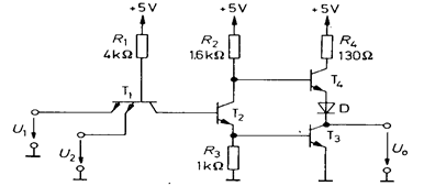
Fig. 1.1 - Standard TTL nand gate, type 7400.
Power dissipation: 10 mW;
Gate propagation delay, tpd = 10ns
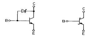
Fig. 1.2 - Transistor with Schottky anti-saturation diode and corresponding circuit symbol.
In TTL circuits, the amplifier consists of drive transistor T2 and a push-pull output stage (totem-pole circuit).
When T2 is conducting, T3 is also on and T4 is off. the output is at L and transistor T3 can accept high currents originating e.g. from the connected gate inputs. (In the L state, a current flows from the inputs!)
When T2 is off, T3 is also off. In this case T4 is turned on and delivers an H signal to the output. The transistor operated as an emitter follower can then supply high output currents and thus rapidly charge up load capacitances. Standard TTL circuits as shown in Fig. 1.1 are no longer used due to the gate propagation delay caused by the saturation of the transistors.
One method of preventing saturation consists of connecting a Schottky diode in parallel with the collector-base junction (Fig. 1.2). When the transistor is conducting, it provides voltage feedback to prevent the collector-emitter voltage falling below about 0.3 V. A TTL gate employing "Schottky transistors" of this type is shown in Fig. 1.3 which is actually a simplified representation of a low-power Schottky TTL gate. Comparison with the standard TTL gate in Fig. 1.1 shows that the values of the circuit resistors are a factor of 5 higher. The power consumption is lower by a factor of 5, being only 2 mW. Nevertheless, the gate propagation delay is no greater, being only 10 ns. The input diode gate, as in DTL circuits, consists of separate diodes. The diode D required in the output stage for level shifting (Fig. 1.1) is here replaced by Darlington pair T3.
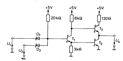
Fig. 1.3 - Low-power Schottky TTL gate, type 74LSOO.
Power dissipation: 2 mW;
Gate propagation delay, tpd = 10ns
The transfer characteristic of the low-power Schottky TTL inverter (not operation) is shown in Fig.1.4 We can see that the switching level is around 1.1 V at the input. The specified tolerance limits are well exceeded: at the maximum permissible L level at the input of 0.8 V, an H level of at least 2.4 V must be present at the output. For the minimum H level at the input of 2.0 V, the L level at the output must be no more than 0.4 V.

Fig. 1.4 - Transfer characteristic of a low-power Schottky TTL inverter.
Hatched areas: Tolerance limits.
Date: 2015-01-12; view: 2706
| <== previous page | | | next page ==> |
| Devices programmed………………………………………………………. 111 | | | Element with the open collector |