CATEGORIES:
BiologyChemistryConstructionCultureEcologyEconomyElectronicsFinanceGeographyHistoryInformaticsLawMathematicsMechanicsMedicineOtherPedagogyPhilosophyPhysicsPolicyPsychologySociologySportTourism
Timing considerations
For a satisfactory operation of the memory, a number of timing conditions must be observed. Figure 3.31 shows the sequence of a write operation. To prevent the data being written into the wrong cell, the write command must not be applied until a certain time has elapsed after definition of the address. This time is called the address setup time tAS . The duration of the write pulse must not be less than the minimum value tWP (write pulse width). The data are read in at the end of the write pulse. They must be valid, i.e. stable, for a minimum period prior to this. This time is called tDW (Data Valid to End of Write). In a number of memories the data and addresses must also be present for a further time tH after the end of the write pulse (Hold Time). As can be seen from Fig. 3.6, the time required to execute a write operation is expressed as
tW = tAS + tWP + tH
This is referred to as the Write Cycle Time.
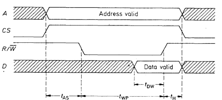
Fig. 3.31 - Timing of a write operation.
tAS = Address Setup Time
tWP = Write Pulse Width
tDW = Data Valid to End of Write Time
tH = Hold Time

Fig. 3.32 - Timing of a read operation.
tAA = Address Access Time
The read operation is shown in Fig. 3.32. After the address is applied, it is necessary to wait for time tAA until the data at the output are valid. This time is referred to as the Address Access Time or simply Access Time.
A list of some of the most widely-used static RAMs in bipolar and CMOS technology is given in Fig. 3.33
| Capacity | Organization | Type | Manufacturer | Operating power, typical | Access time, max. | Pins | |
| CMOS: (VDD =5V, f = fmax) | |||||||
| 16 kbit | 2k x 8 | Hi, Ne, To | 160 mW | 100ns | |||
| 2k x 8 | DS12201 | Da | 250 mW | 150ns | |||
| 4k x4 | Id, Mh, Cy, Is | 225 mW | 15ns | ||||
| 16k x 1 | 200 mW | 12ns | |||||
| 64 kbit | 8k x 8 | Hi, Ne, To | 200 mW | 100ns | |||
| 8k x 8 | DS12251 | Da | 200 mW | 150ns | |||
| 8k x 8 | Id, Mh, Cy, Is | 250 mW | 20ns | ||||
| 4k x 16 | Id, To | 900 mW | 25ns | ||||
| 16k x 4 | Id, Mh, Cy, I | 300 mW | 15ns | ||||
| 64k x 1 | Id, Mh, Cy, Is | 250 mW | 15ns | ||||
| 256 kbit | 32k x 8 | Hi, Ne, To, Fu | 300 mW | 100ns | |||
| 32k x 8 | DS12301 | Da | 300 mW | 150ns | |||
| 32k x 8 | Id, Hi, Ne, Cy, Mh | 250 mW | 35ns | ||||
| 64k x 4 | Id, Hi, Ne, Cy, Mh | 350 mW | 25ns | ||||
| 256k x 1 | Id, Hi, Ne, Cy, Is | 350 mW | 25ns | ||||
| 1 Mbit | 128k x 8 | Hi, Ne, To, Fu | 250 mW | 70ns | |||
| 128k x 8 | DS12451 | Da | 250 mW | 70ns | |||
| 128k x 8 | Id, Hi, Ne | 500 mW | 35ns | ||||
| 256k x 8 | Id, Hi, Ne | 500 mW | 35ns | ||||
| 1024k x 1 | Id, Ne | 500 mW | 35ns | ||||
| 4 Mbit | 512k x 8 | To | 350 mW | 30ns | |||
| 512k x 8 | CYM 14642 | Cy, Id | 1200mW | 45ns | |||
| 256k x 16 | CYM 16412 | Cy.Id | 6000 mW | 25ns | |||
| 8 Mbit | 1024k x 8 | MS810002 | Hm | 300 mW | 85ns | ||
| 256k x 32 | CYM18412 | Cy | 4000 mW | 35ns | |||
| ECL: (VEE = - 5.2 V) | |||||||
| 1 kbit | 256k x 4 | Cy, Ne | 1000 mW | 3 ns | |||
| 4 kbit | 1k x 4 | Cy,Ne | 1200 mW | 3 ns | |||
| 4k x 1 | Fu, Ne | 900 mW | 7 ns | ||||
| 16 kbit | 4k x 4 | Fu, Hi | 1300 mW | 8ns | |||
| 16k x 1 | Fu, Hi, Ne | 1100 mW | 8ns | ||||
| 64 kbit | 16k x 4 | Id, Cy, Fu, Ne, Na | 600 mW | 8ns | |||
| 64k x 1 | Id. Cy, Fu, Ne | 420 mW | 8ns | ||||
| 256 kbit | 64k x 4 | Fu, Na, Hi, Id | 1000 mW | 15ns | |||
| 256k x 1 | Fu, Na, Hi, Ne | 800 mW | 15ns | ||||
Fig. 3.33 - Examples of static RAMs.
1 Containing lithium battery; data retention: 10 years
2 Hybrid circuit (module)
Manufacturers: Cy = Cypress, Da = Dallas, Fu = Fujitsu, Hi = Hitachi, Hm = Hybrid Memory, Id = IDT, Is = Inmos, Mh = Matra Harris, Na = National, Ne = NEC, St = SGS-Thomson, To = Toshiba, Vt = VTI
Date: 2015-01-12; view: 1310
| <== previous page | | | next page ==> |
| Static RAM | | | Dynamic RAMs |