CATEGORIES:
BiologyChemistryConstructionCultureEcologyEconomyElectronicsFinanceGeographyHistoryInformaticsLawMathematicsMechanicsMedicineOtherPedagogyPhilosophyPhysicsPolicyPsychologySociologySportTourism
Shift Registers
A register capable of serial transfer between adjacent cells is called a shift register. It can be shift-right, shift-left, or bidirectional. A typical module has the inputs and outputs indicated in Figure 2.36 and the following description:
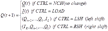
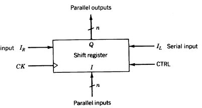
Fig. 2.36 - Bkock diagram of shift register.
The following table illustrates the operations of a 4-bit bidirectional shift register:
| Q | |
| INITIAL | |
| LOAD I= 1110 | |
| LSH IL=0 | |
| LSH IL=1 | |
| RSH IR=0 |
An example of the implementation of n-bit shift register using D flip-flops is shown in Figure 2.37. The coding of the control variables is
| CTRL | C1 | C2 |
| NCH LSH RSH LOAD |
The shift register presented is of the parallel-in /parallel-out type. In some applications shift registers with more limited input and output capabilities are adequate. The use of modules with these reduced capabilities is advantageous because of the reduction in the required number of inputs and outputs. Consequently, for a given number of pins a register with more bits can be implemented. Several type of shift registers exist. We now present some examples.
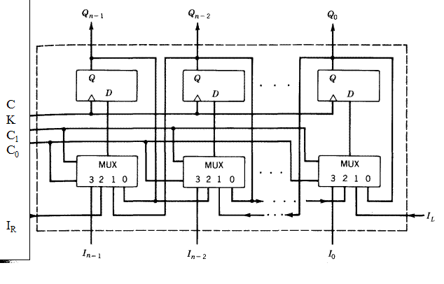
Fig. 2.37 - Implementation of an n-bit shift register.
In a serial-in/serial-out shift register, there is one binary input I and one binary output Q, as shown in Figure 2.38a. If the operation consists of a shift right each clock period, we obtain and so this register can be used as a delay of n clock periods. This type of shift register can be implemented using a package with a small number of pins, independent of the number of cells. This results in a cost-effective module for MSI implementation. It also reduces the interconnection requirements in a VLSI chip.
Q(t)= I(t-n)
A parallel-in/serial-out shift register (Figure 2.38b) has n binary inputs In-1, … , I0 and one binary output Q. If the input is loaded into the register at time t=0 and the register is shifted right each subsequent clock period, the output at time t is
Q(t) = It-1 (0) t>0
A serial-in/parallel-out shift register (Figure 2.38.c) has one binary input I and n outputs Qn-1, . . . , Q0. Again, if a shift right occurs every clock period, the outputs are
Qi(t) = I(t-n+i) i=0, 1, . . . , n-1
The last two types of shift registers are often used to interface digital systems, as shown in Figure 2.39. To keep the interconnection cost low, the n-bit parallel data vector is sent from system A in a bit-serial manner using an n-bit parallel-in/serial-out shift register. The serial n-bit vector is received by system B using an n-bit serial-in/parallel-out shift register.
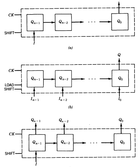
Fig. 2.38 - Types of shift registers, (a) Serial in/serial out. (b) Parallel in/serial out. (c) Serial in/parallel out.
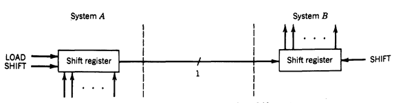
Fig.2.39 - Serial interface using shift register.
Date: 2015-01-12; view: 2045
| <== previous page | | | next page ==> |
| Shift register | | | Counters |