CATEGORIES:
BiologyChemistryConstructionCultureEcologyEconomyElectronicsFinanceGeographyHistoryInformaticsLawMathematicsMechanicsMedicineOtherPedagogyPhilosophyPhysicsPolicyPsychologySociologySportTourism
Power Microprocessors
Power 3.64-bit microprocessor Power 3 was developed by IBM as an alternative to high productivity processors Intel and Alpha and was intended for using in high productivity servers and workstations. The presence of supporting means for multiprocessor mode allows using it in SMP-systems.
??w?r 3 is a superscalar microprocessor with extraordinary speculative instruction execution. During one cycle ??w?r 3 is capable to perform up to 8 instructions: 2 instructions of Load/Store, 2 instruction with floating point, 2 short integer instructions, 1 long integer instruction, and 1 branch instruction.
The structure of the microprocessor is shown in Fig. 6.5.
??w?r 3 contains 7 executive units: 2 with floating point (FPU), 3 with fixed point (F?U), 2 units for load and store (L/St).
The processor contains a separate cache memory of the first level; a cache for data up to 64 Kbytes, and a cache for instructions up to 32 Kbytes. The data and instructions caches have nonblocking associative sets of 128 inputs. ??w?r 3 may use cache-memory of the second level with capacity of 1 through 16 Mbytes, which is connected to the separated 256-bit bus, working with 200 MHz. The transfer speed with the cache of the second level is 6.4 Gbytes/s. The transfer with the main memory is accomplished via 128-bit system bus using clock pulses of 100 MHz. 'The transfer speed is 1.6 Gbytes/s.
 The peculiarity of the processor is its minimal time for starting instruction execution ? only 3 cycles, which decreases the pipeline latency in the case of the branch wrong prediction. The microprocessor contains 15 millions transistors on the chip.
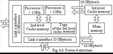
 Power 4.64-bit microprocessor ??w?r 4 is a 2-processor system on one chip (Fig. 6.6). ??w?r 4 contains also a large die cache memory, high-speed port for outer memory, and links for uniting microprocessors into DS? (Distributed Shared Memory) system.
Besides Instructions Level Parallelism (IL?), the processor uses also Thread Level Parallelism (?L?).
Each of the placed on the chip processor is a superscalar one with unordered and speculated instruction execution. Up to 8 instructions may be chosen simultaneously, more than 200 instructions are considered for execution, and 8 instructions are executed in 8 functional units.
The processor functional units are: 2 units with floating point (F?), 2 units with fixed point (FX), 2 units for loading/store (LD/ST), 1 unit for branching (?R), and 1 unit for logical operations (?P). On average, 5 instructions are executed in each processor during one cycle.
The processor execution pipeline is shown in Fig. 6.7. Stages IF (Instruction Fetching), I? (placing Instruction into Cache-memory), and ?? (Branch Prediction) are used while loading the next instruction. Stages D0 through GD are used while instruction decoding and grouping (in queues to the functional units). Stages ?? are used for determining dependencies between instructions, fixing resources, and setting instructions in queues to the appropriate functional units. The further processing is fulfilled in the four independently functioning pipelines.

Stages ISS (Instruction-Set Simulator) through W? are used for instruction fulfillment, beginning with the instruction fetching from the queue and finishing with storing results into the register file.
Stages ?fer and ?? are used for checking the fulfillment of the all previous instructions (in accordance with their ordered numbers in the program) and outing the result.
The processors contain separate caches for instructions and data of the first level with each volume of 64 Kbytes. The distributed by processors on-chip cache-memory of the second level (8-inputs associative set with volume of 1.5 Mbytes), controller, and tag memory of the outer cache-memory of the third level are placed on the chip.
For connection the cache-memory of the third level with volume of 32 Mbytes there is a two-directed port with capacity of 16 bytes, functioning with 1/3 of the processor clock rate providing throughput of 10 Gbytes/s.
For forming multiprocessing configurations there are 3 links with total throughput of 35 Gbytes/s.
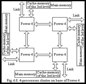
Fig. 6.8 shows 4-processor system based on ??w?r 4.
The microprocessor has I?? IS? instruction set, realized in RS/6000 and ?S/400 and it is completely compatible with ??w?r?? instruction system.

Basic Alternatives, Possible Implementation Schemes.Theoretically in the design space of register renaming, each possible combination of the available design choices yields one possible implementation alternative. However, instead of considering all possible implementation alternatives, it makes sense to focus only on those that differ in relevant qualitative aspects from each other ? the basic alternatives. Poss-ible basic alternatives can be derived from the design space in two steps: by identifying the relevant qualitative design aspects involved and then by composing their possible combinations. When selecting the relevant qualitative design aspects, we should recall the design space of renaming mentioned earlier. First, we ignore two main aspects: the scope of register renaming because recent processors typically implement full renaming, and the rename rate because of its quantitative character. Two main design aspects remain: the layout of the rename buffers and the method of register mapping. Furthermore, the layout of the rename buffers itself covers three design aspects: the type of rename buffers, their number, and the number of the read and write ports. Of these only the type of the rename buffers is of qualitative character. It follows that the design space of register renaming includes only two relevant qualitative aspects: the type of the rename buffers and the method of register mapping.
The design choices available for these two relevant design aspects result in eight possible combinations, called the basic alternatives for register renaming, as shown in Fig. 6.9. In addition, this figure also takes into account that the processor's operands fetch policy ? which is a design aspect of shelving ? significantly affects how the renaming process is carried out. This splits the eight basic renaming alternatives into 16 feasible implementation schemes. Fig. 6.9 also indicates which implementation schemes are used in relevant superscalar processors and some hints about their origins. As Fig. 6.9 indicates, relevant superscalar processors make use of only four of the eight possible basic alternatives of renaming. Moreover, most of the latest processors employ the following basic alternatives of renaming when fetching dispatch-bound operands: use of merged architectural and rename register files and mapping tables (R10000, R12000, M3); use of separate rename register files and mapping registers within the rename registers (PA8x00 line, Power3); and renaming within the ROB and using mapping tables (Pentium Pro, PentiumII, Pentium III, Pentium IV).

It is also conceivable to use different basic alternatives for renaming fixed-point and floating-point instructions, as is done in the K7. This processor uses the ROB for renaming fixed-point instructions and a merged architectural and rename register file for renaming floating-point ones. However, as AMD didn't disclose the method of register mapping, this processor is not included in Fig. 6.9. As this figure shows, the latest processors fetch predominantly dispatch-bound operands due to the comparative advantage of this fetch policy. The move away from the issue-bound operands to the dispatch-bound fetch policy is manifested in AMD's subsequent K5 and K6, and by the fact that the PowerPC 620-based Power3 has also made this transition.
Register renaming and shelving mark the first major step in the evolution of superscalar processors. The introduction of these techniques became necessary to resolve the issue bottleneck of early superscalar designs. As revealed here, register renaming is a complex technique whose understanding requires the identification and exploration of its design space.
Date: 2016-06-12; view: 382
| <== previous page | | | next page ==> |
| Questions for Self-Testing | | | Microarchitecture Level Power-Performance Fundamentals |