CATEGORIES:
BiologyChemistryConstructionCultureEcologyEconomyElectronicsFinanceGeographyHistoryInformaticsLawMathematicsMechanicsMedicineOtherPedagogyPhilosophyPhysicsPolicyPsychologySociologySportTourism
RAMs as shift registers
RAMs can be operated as shift registers if the addresses are applied cyclically. The counter shown in Fig. 3.7 is used for this purpose. For each address, the stored data are first read out and new data are then read in. The timing diagram is shown in Fig. 3.8. The positive-going edge of the signal increments the counter. If the CLK signal is simultaneously used as the R/  signal, the memory contents are then read out and stored in the output flip-flop on the negative-going edge. While CLK = 0, the new data Din are written into the memory cell which has just been read out. In this case the minimum clock cycle is shorter than the sum of the read and write cycle times, since the address remains constant. It is equal to what is known as the "Read-Modify-Write Cycle Time".
The difference between this type of shift register and the normal type is that only the address, which acts as a pointer to the fixed data, is shifted, not the data themselves. The advantage of this method is that normal RAMs can be employed, and these are obtainable with memory capacities far greater than those of normal shift registers. If the clock frequency is higher than 64 kHz, dynamic 1 Mbit-RAMs can even be used without refresh logic, since this frequency ensures that the lowest 512 addresses are processed in 8 ms.
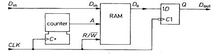
Fig. 3.7 - RAM operatedas a shift register.
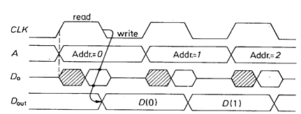
Fig. 3.8 - Timing diagram for a RAM shift register.
Even at high shift frequencies, low-cost RAMs can still be used if several data bits are processed in parallel and a serial-parallel converter is provided at the input and a parallel-serial converter at the output, in order to obtain the required shift frequency.
First-In-First-Out Memories (FIFOs)
A FIFO is a special type of shift register. The common feature is that the data appear at the output in the same order as they were read in: the first word read in is also the first one read out. With a FIFO, as opposed to a shift register, this process can take place completely asynchronously, i.e. the read-out clock is independent of the read-in clock. FIFOs are therefore used for linking asynchronous systems [3.6].
Operation is very similar to that of a waiting line: the data do not move at a fixed rate from input to output, but only remain in the register long enough for all the previous data to be read out. This is shown schematically in Fig. 3.9. With first-generation FIFOs, the data were actually shifted through a register chain, as illustrated in Fig. 3.9. On entry, the data were passed on to the lowest free memory location and shifted onwards from there to the output by the read clock. One disadvantage of this principle was the long fall-through time. This is particularly noticeable when the FIFO is empty, as the input data then have to pass through all the registers before being available at the output. This means that even the smallest FIFOs exhibit fall-through times of several microseconds. Other disadvantages include the complex shift logic and the large lumber of shift operations, thereby precluding a current-saving implementation in CMOS technology.
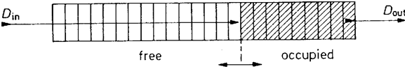
Fig. 3.9 - Schematic diagram of FIFO operation.
To overcome these drawbacks, in the second-generation FIFOs it is no longer the data that are shifted, but merely two pointers which specify the input and output address in a RAM. This is illustrated in Fig. 3.10. The input counter points to the first free address Ain, the output counter to the last occupied address Aout. Both pointers therefore rotate during on-going data input and output.
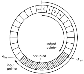
Fig. 3.10 - FIFO as ring memory.
The distance between the two pointers indicates how full the FIFO is. When Ain – Aout = Amax, the FIFO is full. No more data must then be entered, as this would mean overwriting data which have not yet been read out. When Ain = Aout, the FIFO is empty. No data must now be read out, as this would mean receiving old data a second time. An overflow or empty condition can only be avoided if the average data rates for input and output are identical. To achieve this, it is necessary to monitor the occupancy of the FIFO and to attempt to control the source or sink in such a way that the FIFO is on average half full. The FIFO can then accommodate short-term fluctuations, assuming it has a sufficient storage capacity.
The design of a FIFO is shown in Fig. 3.11. It is similar to the RAM shift register in Fig. 3.7. Read-while-write memories with separate address inputs (see Fig. 3.4) are particularly suitable here, as reading and writing can occur asynchronously. The more recent FIFOs, examples of which are listed in Fig. 3.12, operate on this principle.
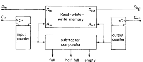
Fig.3.11 - FIFO implementation with read-while-write memory.
| Capacity | Organization | Type | Manufacturer | Operating power, typical | Clock frequency max | Pin | |||
| Standard FIFOs, (MOS: VDD = 5 V, f = fmax) | |||||||||
| 320 bit | 64x5 | IDT 72404 | Id, Am, Cy | 175 mW | 45MHz | ||||
| 576 bit | 64 x 9 | CY7C409A | Cy | 350 mW | 35MHz | ||||
| 2 kbit | 256 x 9 | IDT 7200 | Id, Am | 300 mW | 40MHz | ||||
| 5 kbit | 512 x 9 | IDT 7201 | Id, Am, Cy, Da, St | 300 mW | 40MHz | ||||
| 9 kbit | 1k x 9 | IDT 7202 | Id, Am, Cy, Da, St | 300 mW | 40MHz | ||||
| 18 kbit | 2k x 9 | IDT 7203 | Id, Am, Cy, Da, St | 375 mW | 30MHz | ||||
| 36 kbit | 4k x 9 | IDT 7204 | Id, Da | 375 mW | 30MHz | ||||
| 36 kbit | 4k x 9 | IDT 72B04 | Id | 65 MHz | |||||
| 72 kbit | 8k x 9 | IDT 7205 | Id | 20MHz | |||||
| 72 kbit | 4k x 18 | IDT 72045 | Id | 20MHz | |||||
| 144 kbit | 16k x 9 | IDT 7206 | Id | 20MHz | |||||
| 144 kbit | 8k x 18 | IDT 72055 | Id | 20MHz | |||||
| 256 kbit | 32k x 8 | UPD425321, 2 | Ne | 300 mW | 10 MHz | ||||
| 1 Mbit | 256k x 4 | TMS4C10501 | Ti | 250 mW | 20MHz | ||||
| Bidirectional FIFOs, CMOS: (VDD = 5 V, f = fmax) | |||||||||
| 9 kbit | 512 x 9 | 67C4701 | Am | 350 mW | 16MHz | ||||
| 512 x 18 | IDT 72511 | Id | 450 mW | 30MHz | |||||
| 36 kbit | 1k x 18 | IDT 72521 | Id | • 350 mW | 30MHz | ||||
Fig. 3.12 - Examples of FIFOs.
1 Contains dynamic RAM
2 Refresh controller integrated
Manufacturers: Am = AMD, Cy = Cypress, Da = Dallas, Id = IDT, Ne = NEC, St = SGS-Thomson, Ti = Texas Instr.
Date: 2015-01-12; view: 1758
| <== previous page | | | next page ==> |
| Mask-type LIC of the ROM | | | FIFO implementation using standard RAMs |