CATEGORIES:
BiologyChemistryConstructionCultureEcologyEconomyElectronicsFinanceGeographyHistoryInformaticsLawMathematicsMechanicsMedicineOtherPedagogyPhilosophyPhysicsPolicyPsychologySociologySportTourism
Static RAM
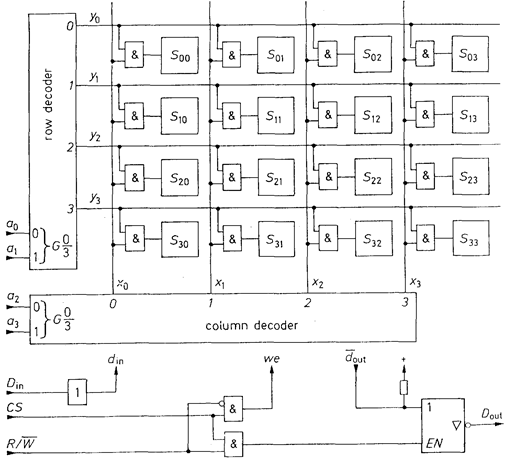
A RAM is a memory device in which data can be stored under a specified address and subsequently read out from that address (random access). For technological reasons the individual memory cells are not arranged linearly but in a square matrix. To select a particular memory cell, address A is decoded, as shown in Fig. 3.28, by a row and column decoder.
Fig. 3.28- Internal structure of a RAM. Example showing 16-bit memory capacity.
Din = Data input Dout = Data output CS = Chip Select R/
we = write enable
In addition to its address inputs, a RAM has an extra data input Din, a data output Dout, a read/write pin R/ During the write process (R/ Another logic operation prevents a switchover to the write state (we = 1), if CS = 0. This prevents data being written accidentally until the relevant memory has been selected. Figure 3.28 shows the logic operations mentioned above. Lines din, dout and we (write enable) are connected to each memory cell internally, as illustrated schematically in Fig. 3.29. Data should only be read into the memory cell when address condition xi = yi = 1 is satisfied and also we = 1. This logic operation is performed by gate G1. The contents of the memory cell must only reach the output if the address condition is satisfied. This operation is performed by gate G2, which has an open-collector output. When the cell is not addressed, the output transistor is off. The outputs of all the cells are internally wire-ANDed together and connected to the memory output Dout via the tristate gate shown in Fig. 3.28.
Fig. 3.29 - Equivalent logic circuit for the structure of a memory cell.
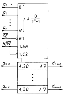
Unless the supply voltage is switched off, the memory contents are retained until they are modified by a write command. Such memories are referred to as static to distinguish them from dynamic memories in which the contents have to be refreshed at regular intervals to prevent them from being lost. The circuit symbol for a RAM is shown in Fig. 3.30. As we can see, there are N address inputs. These are decoded by the address decoder in such a way that precisely that memory cell is selected (out of 2N) which corresponds to the address applied. The read-write changeover R/ Frequently, not just a single bit, but an m-digit word is stored at an address. The storage of entire words may be seen as a spatial extension of the block diagram in Fig. 3.28. The additional bits are then stacked in further memory layers; their control lines x, y and we are connected in parallel, and their data lines form the input or output word.
Fig. 3.30 - RAM circuit symbol.
Date: 2015-01-12; view: 2604
|
 = Read/Write
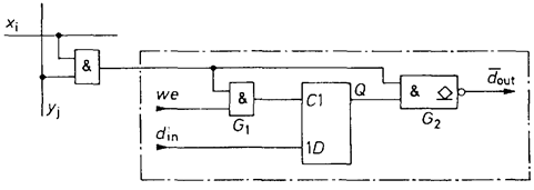
 = 0. The tristate output is therefore activated for R/