CATEGORIES:
BiologyChemistryConstructionCultureEcologyEconomyElectronicsFinanceGeographyHistoryInformaticsLawMathematicsMechanicsMedicineOtherPedagogyPhilosophyPhysicsPolicyPsychologySociologySportTourism
Synchronous BCD counter
The synchronous decade counter in Fig. 2.61 has largely similar circuitry to the synchronous straight binary counter in Fig. 2.59. As with the asynchronous decade counter, two additional features are again required to ensure that, at the transition from 9 = 10012 to Odec = 0000, flip-flop F3 changes state and not flip-flop Fj. The disabling of F, is achieved in Fig. 2.61. via the feedback path of Q3, the change of state of F3 by additionally decoding the 9 at the toggle control input.
Examples of synchronous BCD counters: 74 LS160 (TTL); 4160 (CMOS);
with up-down control:
74LS190(TTL); 10137 (ECL); 4510 (CMOS);
with up/down clock input:
74 LSI 92 (TTL)
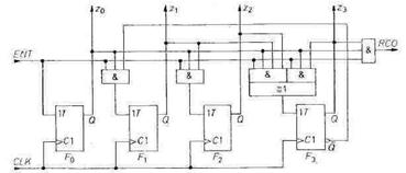
Fig. 2.61 - Synchronous BCD counter.
Synchronous one-shot
It is possible, using the circuit in Fig. 2.62, to generate a pulse which is in synchronism with the clock. The pulse length equals one clock period and is independent of the length of the trigger signal x,
If x changes from 0 to 1, Q1 = i at the positive-going edge of the next clock pulse, i.e. y = 1. On the subsequent leading edge, Q2 becomes 0 and y becomes 0 again. This state remains unchanged until x has been zero for at least one clock period and has returned to 1. Short trigger pulses which are not registered by the leading edge of a clock pulse are lost, as with the synchroni/ing circuit
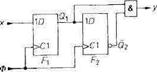
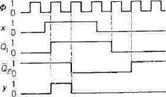
Fig. 2.62 - Generation of a single, but Fig. 2.63 -Timing diagram.
clock-synchronous pulse.
If they too are to be considered, an additional flip-flop must store the pulses until they are transferred to the main flip-flop. The timing diagram in Fig. 2.63 shows an example of operation. A synchronous one-shot for ON-times longer than one clock period can be realized quite simply by using a synchronous counter, as is shown in Fig. 2.64. If the trigger variable X is at 1, the counter is loaded in the parallel-in mode on the next clock pulse. The following clock pulses are used to count to the maximum output state Zmax. At this number, the carry output RCO — 1. The counter \* then inhibited via count-enable input ENP; the output variable y is 0. The ordinary enable input ENT cannot be employed for this purpose as it not only affects the flip-flops but also RCO directly, and this would result in an unwanted oscillation.
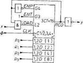
Fig. 2.64 - Synchronous one-shot.
A new cycle is started by parallel read-in. immediately after loading, RCO becomes zero and v is then 1. The feedback from RCO to the and gate at the x-input prevents a new loading process unless the counter-has reached the state Zmas. By this time, x should have returned to 0; if not, the counter is loaded again, i.e. is operating as a modulo-(M 4- 1) counter as The timing diagram is shown in Fig. 2.65 for an ON-time of 7 clock pulses. If a 4-bit straight binary counter is employed, it must, for this particular ON-time, be loaded with P = 8. The first clock pulse is needed for the loading process and the remaining 6 pulses for counting up to 15.
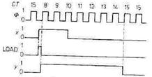
Fig. 2.65 -Timing diagram CT= Content.
Synchronous edge detector
A synchronous edge detector gives an output signal in synchronism with the clock pulse whenever the input variable x has changed. For the implementation of such an arrangement, we consider the one-shot circuit in Fig. 2.62. It produces an output pulse whenever x changes from 0 to 1. In order that a pulse is also obtained at the transition from 1 to 0, the and gate must be replaced by an exclusive-oR gate, producing the circuit in Fig. 2.66. Its characteristics are illustrated by the timing diagram in Fig, 2.67.
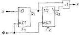
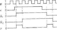
Fig. 2.66 - Synchronous edge detector. Fig. 2.67 - Timing diagram.
Synchronous clock switch
The problem often arises of how to switch the clock on and off without interrupting the clock pulse generator. In principle, an and gate could be used for this purpose, but this would result in the first and the last pulse being of undefined length if the switching signal is not clock-synchronized. This effect can be avoided by employing a single-edge triggered D-type flip-flop for the synchronization, as is shown in Fig. 2.68. If EN = 1, at the next leading pulse edge Q = 1 and therefore <t>' = 1. The first pulse of the switched clock <t>' always has the full length because of the edge-triggering property.
The leading pulse edge cannot be used to switch off since, directly after the transition, Q = 0, which would result in a very short output pulse. The flip-flop is therefore cleared asynchronously via the reset input when EN and <P are 0, achieved by the nor gate at the R-input. As is obvious from Fig. 2.69, only full-length clock pulses can reach the output of the and gate.
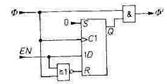
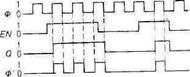
Fig. 2.68 - Synchronous clock switch. Fig. 2.69 - Timing diagram.
Date: 2015-01-12; view: 1683
| <== previous page | | | next page ==> |
| Synchronous reversal counters | | | Schmitt flip-flops |