CATEGORIES:
BiologyChemistryConstructionCultureEcologyEconomyElectronicsFinanceGeographyHistoryInformaticsLawMathematicsMechanicsMedicineOtherPedagogyPhilosophyPhysicsPolicyPsychologySociologySportTourism
Flips types
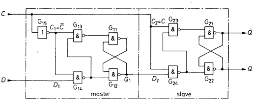
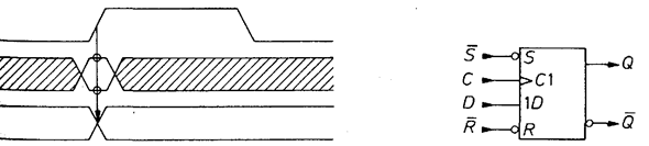
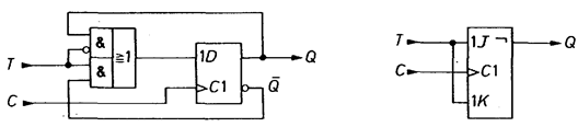
Single-edge-triggered flip-flops Flip-flops with intermediate storage can also be implemented by connecting two transparent D flip-flops (Fig. 2.10) in series and clocking them with complementary signals. This produces the circuit shown in Fig. 2.18. As long as lock C = 0, the master follows the input signal and we have Q1 = D. The slave meanwhile stores the old state. When the clock goes to 1, the data D present at that instant is frozen in the master and transferred to the slave and thus to the Q output. The information present at the D input on the positive-going edge of the clock signal is therefore instantaneously transmitted to the Q output. The state of the D input has no effect for the rest of the time. This can also be seen from Fig. 2.19. Instead of waiting for the negative-going edge, as in the JK flip-flop with data lockout, the input value appears at the output immediately. For this reason, the circuit symbol in Fig. 2.20 also has no delay symbols. This constitutes a significant advantage, in that the entire clock cycle is now available for forming the new D signal. If JK flip-flops are used, this process must take place while the clock is zero, i.e. with symmetrical clock pulses in half the time.
Examples of IC types:
74LS74(TTL); 10131 (ECL); 4013 (CMOS)
Fig. 2.18 - Single-edge-triggered D flip-flop.
Fig. 2.19 - Timing diagram for the input and Fig. 2.20 - Circuit symbol for the output signals in thesingle-edge-triggered triggered D flip-flop. D flip-flop.
Single-edge-triggered D flip-flops can also be operated as toggle flip-flops. For this purpose we make D = It is also possible to make the inversion dependent on a control variable by providing feedback from either
Fig. 2.21 - Single-edge-triggered D flip-flop Fig. 2.22 - Timing pattern in the as a frequency divider. frequency divider.
It is also possible to make the inversion dependent on a control variable by providing feedback from either
Fig. 2.23-24 - Controllable toggle flip-flops.
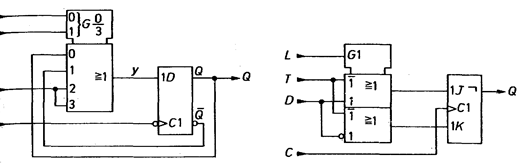
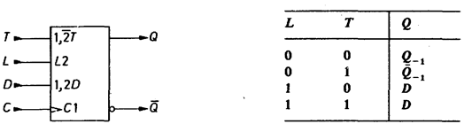
Multi-purpose flip-flops can be obtained by additionally providing synchronous data input. The multiplexer can then be given another input preceding the D input. This additional input is selected via Load input L as shown in Fig. 2.25. If L = 1, then y = D and therefore, after the next clock signal, Q = D. When L = 0, the circuit operates in exactly the same way as that in Fig. 2.23. The mode of operation of this multifunction flip-flop is summarized in Fig.2.27. The same behavior can also be obtained using a JK flip-flop as shown in Fig. 2.26. When L = 1, J = D or K = Due to their versatility, the multifunction flip-flops in Figs. 2.25-26 constitute the basic building blocks of counters.
Figs. 2.25-26 - Multifunction flip-flops.
T = Toggle, L = Load, D = Data, C = Clock
Fig. 2.27a - Circuit symbol of a multifunction Fig. 2.27b - Function table of a flip-flop. multifunction flip-flop.
Date: 2015-01-12; view: 1300
|
 as in Fig. 2.21. The output state therefore inverts at each positive-going edge of the clock signal. This is illustrated in Fig. 2.22. If transparent D flip-flops were used, an oscillation would be obtained while clock C = 1, instead of a frequency division. It is caused by the transparent propagation of the signal through the circuit, resulting in a signal inversion after every propagation delay time.
 for
for 
 . Therefore, after the next clock signal, Q = D. When L = 0, we have J = K = T; the circuit then operates as in Fig. 2.24. In the case of JK flip-flops, it must be remembered that the data have to be present before the positive-going edge of the clock signal, but only appear after the output on the negative-going edge. With normal JK flip-flops (as in Fig. 2.13), it must also be ensured that the J and K inputs do not change as long as C = 1. During this time the L, T and D inputs must therefore also remain unchanged.