CATEGORIES:
BiologyChemistryConstructionCultureEcologyEconomyElectronicsFinanceGeographyHistoryInformaticsLawMathematicsMechanicsMedicineOtherPedagogyPhilosophyPhysicsPolicyPsychologySociologySportTourism
Emitter-coupled logic (ECL)
We saw in a differential amplifier with an input voltage difference of about ± 100 mV, current Ik can be completely switched from one transistor to the other. The amplifier therefore possesses two defined switching states, namely /c = 1k or /c = 0. It is therefore also known as a current switch. If, for this switch mode, suitably low-resistance components are selected to ensure that the change in voltage across the collector resistors remains sufficiently low, the conducting transistor can be prevented from being driven into saturation.
Figure 1.10 shows a typical ECL gate. Transistors T2 and T3 form a differential amplifier. A constant potential Vref is applied to the base of T3 via the voltage divider. If all the input voltages are in the L state, transistors T1 and T2 are turned off. The emitter current in this case flows via transistor T3, producing a voltage drop across R2 . Output voltage U01 is therefore in the L state, U02 in the H state. When at least one input level goes high, the output states are reversed. Positive logic gives an or operation for U01 and an nor operation for U02 .
We shall now examine the potentials within the circuit. When transistor T3 is off, only a small voltage of about 0.2 V is dropped across R2 , due to the base current of T5 . Consequently the emitter potential of T5 is in this case -0.9 V.
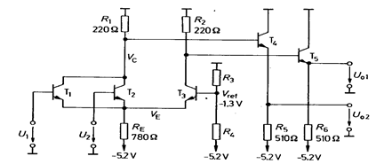
Fig. 1.10 - ECL nor-or gate, type MC10102. Emitter resistors R5 and R6
are not incorporated in the IC and must be connected externally if required/
Power dissipation per gate-. 25 mW
Power dissipation R5, R6 , each: 30 mW
Gate propagation delay, tp, = 2 ns
This is the output H level. If this level is applied e.g. to the base of T2 , the emitter potential is
VE= -0.9V-0.7V = -1.6V .
In order to ensure that T2 is not driven into saturation, its collector-emitter voltage must not fall below 0.6 V. Consequently, the minimum collector potential is
Vc= -1.6V+0.6V = -1.0V .
This produces an L level at the output of-1.7 V. Vref must now be selected such that the input transistors are sure to be on at an input voltage of UH = -0.9V and off at an input voltage of UL = -1.7V. This condition can best be satisfied by setting Vref half-way between UH and UL, i.e. at about - 1.3 V. The complete transfer characteristic is shown in Fig. 1.11. We can see that the switching level is -1.3 V. At the maximum permissible input L level of - 1.5 V, an H level of at least - 1.0 V must be produced at the nor output. At the lowest input H level of -1.1 V, the L level at the output must not exceed -1.65 V.
In contrast to other logic circuit families, the input voltage of ECL in the H state is tightly constrained at the upper limit. If it exceeds - 0.8 V, the relevant input transistor will be driven into saturation. This can be seen from the bend .in the transfer characteristic for the nor output, at - 0.4 V input voltage. As the voltage increases further, the collector potential VC increases with the emitter potential due to the saturation of transistor T2, and therefore output voltage U02 also increases.
We can see from Fig. 1.11 that the logic levels are much closer to zero potential than to the negative supply voltage ( - 5.2 V). Moreover, the magnitude of the supply voltage does not affect the H level, as this is determined only by the base-emitter voltage of the emitter followers. If the negative terminal of the supply voltage had been made zero potential, i.e. the level reference, +5.2V would be superimposed on all the levels. In view of the low switching levels, reliable operation would be impossible
Of all the logic families, ECL circuits have the smallest gate propagation delays. Indeed, they are even faster than Schottky TTL circuits which can also be operated unsaturated. The difference is that the collector-emitter voltage across the conducting transistors is higher - never less than 0.6 V. This provides not only a greater margin to the saturation voltage, but also results in a lower collector-base junction capacitance.
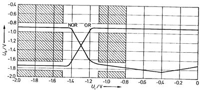
Fig. 1.11 - Transfer characteristic of an ECL gate of the MC10000 series.
Hatched areas: Tolerance limits.
Another reason for the high speed of ECL circuits ,lies in the small signal amplitudes of only 0.8 V involved in switching. The unavoidable switching capacitances can therefore be reverse-charged rapidly. The low output resistance of the emitter followers also promotes fast switching times. From Eq. (4.30) this is given by

The high speed of ECL circuits is obtained at the expense of high power dissipation. For a gate of the MC 10.000 series this can be as much as 25 mW. To this must be added the power dissipation in the emitter resistors. For an average output voltage of - 1.3 V, there is a power dissipation of 30 mW in a 51012 emitter resistor, i.e. more than in the entire gate. For this reason emitter resistors will only be connected to the outputs used. The dissipation in the emitter resistors can be reduced to 10 mW if, instead of connecting 510 fi resistors to the - 5.2 V supply, 50 fi resistors are used on an additional supply voltage of VTT = -2 V. However, the associated cost and complexity is only justifiable for extensive ECL circuitry. Additional care must be taken to ensure that the -2V supply voltage is generated with high efficiency in the power supply. Otherwise the problem of power dissipation is merely shifted from the circuit to the power supply. For this reason it is impractical to produce the -2V from the - 5.2 V using a series regulator.
Emitter-coupled Schmitt trigger
A non-inverting amplifier can also be implemented by using a differential amplifier. By applying positive feedback through a resistive voltage divider, we obtain the emitter-coupled Schmitt trigger shown in Fig.1.12. Both of its trigger thresholds are positive.
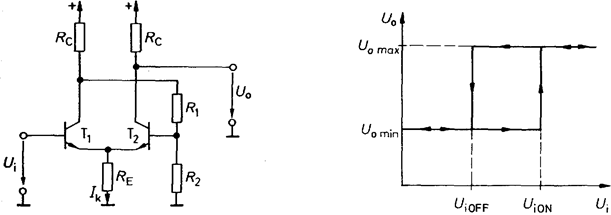
Fig. 1.12 - Emitter-coupled Schmitt trigger . Fig. 1.13 - Transfer characteristic.
By selecting suitable component values for the circuit, we can cause current IK to switch from one transistor to the other when the circuit changes state, without the transistors becoming saturated. This eliminates the storage time tS during switchover, and very high switching frequencies can be achieved. This principle is known as "unsaturated logic".
Date: 2015-01-12; view: 3647
| <== previous page | | | next page ==> |
| Tristate outputs | | | Emitter-coupled multivibrator |