CATEGORIES:
BiologyChemistryConstructionCultureEcologyEconomyElectronicsFinanceGeographyHistoryInformaticsLawMathematicsMechanicsMedicineOtherPedagogyPhilosophyPhysicsPolicyPsychologySociologySportTourism
Complete the sentences.1. Photoconduction has been an important tool 2. Photoconducting devices are used to 3. Photoconductive devices normallyhave 4. are used to measure the resistance of the photoconductor. 5. Photoconduction has been observed in Make up word combinations from the following words.
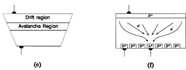
Translate into Ukrainian words and word combinations (task 6) 9. Put the following words into correct order to make sentences: 1. and Indium antimonide the 4- and 10-mm semiconductors mercury-cadmium-telluride provide photosensitivity range in wavelength . 2. The energy photon for this excitation has the of bandgap the semiconductor to exceed. 3. in has been observed single-crystalline materials Photoconduction amorphous, polycrystalline, and. 10. Supply the correct form of the adjectives and adverbs in parentheses. Let asandthanbe your clues. Add any other words that may be necessary. 1. John and his friends left(soon) as the professor had finished his lecture. 2. His job is(important) than his friend's. 3. He plays the guitar (well) as Andres Segoria. 4. A new house is much(expensive) than the older one. 5. Last week was(hot) as this week. 6. Martha is(talented) than her cousin. 7. Bill's descriptions are(colourful) than his wife's. 8. Nobody is(happy) than Maria Elena. 9. The boys felt(bad) than the girls about losing the game. 10. A grey hound runs(fast) than a chihuahua. Read and translate text B. Text B Photojunction sensors. Photojunction sensors (photodiodes and phototransistors) are semiconductor devices that convert the electrons generated by the photoelectric effect into a detectable electronic signal. The photoelectric effect is a phenomenon in which photons lose energy to electrons in a material. In the case of a semiconductor, when the energy of an interacting photon (hn) exceeds the energy of the semiconductor bandgap (Eg), the energy absorbed can promote an electron from the valence band to the conduction band of the material. This causes the formation of an electron-hole pair. In the presence of an electric field, these charges drift toward electrodes on the surface and produce the signal. The junction in the photojunction device creates a diode that provides a small built-in electric field to propel the charges to the electrodes (photovoltaic mode of operation). In the photovoltaic mode, either the photocurrent or the photovoltage can be measured. This mode of operation provides very high sensitivity because there is no net reverse leakage current, but relatively poor frequency response occurs because of high capacitance and low electric field. Photodiode devices are most often operated with a bias voltage applied opposing the junction (reversed bias) to provide the electric field. The presence of the junction in a diode allows for the application of a relatively large bias to be applied while maintaining a relatively low reverse leakage current and thus relatively low noise. The result of an applied bias on a junction is the increase of the “depletion region,” which is the sensitive volume of the detector. Any charges that are generated within this volume are swept toward the electrodes by the field, adding to the reverse leakage current. The total reverse current is the sum of the dark current, which occurs due to thermal generation of charges in the depletion region, and the photocurrent, which is produced due to optical illumination. Thus, the lower the dark current, the higher the sensitivity of the detector to optical illumination. In an ideal diode, the entire light incident on the photodiode surface is converted to electron-hole pairs and all of the charges drift to the electrodes and are collected. In a real device, there are reflection losses at the surface, additional light is lost in the electrode and/or front layers of the device, and not all of the charges are collected at the electrodes. There are several fundamental types of junction photodiodes, as shown in Figure 17.1. A Schottky barrier diode is a device in which the junction is formed at the surface of the semiconductor by the application of a metal electrode that has a work function that is different from the work function of the semiconductor; a heterojunction diode is a device in which two different semiconductor materials with differing work functions are joined; a homojunction diode is a device in which the junction is created at an interface in a single material and the difference in work function is created by doping the material n-type and p-type. Most photodiodes are homojunction devices made using silicon. Other, more complex types of photojunction devices, which are discussed below, include p-i-n photodiodes, avalanche photodiodes (APD), drift photodiodes, and phototransistors.
Figure 17.1 Schematic of photodiode device structures: (a) Schottky junction, (b) homojunction, (c) heterojunction, (d) p-i-n, (e) APD, (f) drift diode.
Photodiodes are typically characterized by several properties, including bandwidth, spectral response, operating bias, operating temperature, dark current, junction capacitance, noise equivalent power, and peak wavelength. Other specifications usually provided by manufacturers include size, packaging details, operating temperature range, capacitance, and price. Photodiodes are used in numerous applications, including CD-ROM systems, television remote control systems, fax machines, copiers, optical scanners, fiber optic telecommunication repeaters, surveillance systems such as motion detectors, certain smoke detectors, light meters, and a wide variety of scientific instrumentation including spectrophotometers, scintillation detectors, optical trackers, laser range finders, LIDAR, LADAR, analytical instrumentation, optical thermometers, nephelometers, densitometers, radiometers laser detectors, shaft encoders, and proximity sensors. Photodiode arrays are available for use as position-sensitive detectors that can either be used for imaging (such as in laser scanners, night vision equipment, spectrophotometers, and edge detection) or alignment systems. Medical imaging applications such as x-ray CT scanners also use large arrays of photodiodes. Photodiodes are an alternative to photomultiplier tubes in many applications. There are a variety of advantages to be gained - including higher quantum efficiency, tailored spectral response, increased ruggedness, reduced power requirements, reduced weight, compact size, elimination of warm-up period, reduced sensitivity to temperature and voltage fluctuations, and insensitivity to magnetic fields. In general, photodiodes are noisier and require more sophisticated readout electronics than photomultiplier tubes, especially at room temperature. Upon cooling, the noise in photodiodes can be reduced significantly due to reduction in dark current. 12. Complete the table:
13.Find in the text equivalents to the following words and expressions: 1. the state or quality of being sensitive (s_ _ _ _ _ _ _ _ _y) 2. instability, constant change (f_ _ _ _ _ _ _ _ _n) 3. a long hollow and typically cylindrical object (t_ _ _) 4. the quality or state of being efficient (e_ _ _ _ _ _ _cy) 5. a semiconductor diode, the conductivity of which is controlled by incident illumination (ph_ _ _ _ _ _ _e) Date: 2016-04-22; view: 766
|