CATEGORIES:
BiologyChemistryConstructionCultureEcologyEconomyElectronicsFinanceGeographyHistoryInformaticsLawMathematicsMechanicsMedicineOtherPedagogyPhilosophyPhysicsPolicyPsychologySociologySportTourism
Energy bands and electrical conductionExplaining semiconductor energy bands There are three popular ways to classify the electronic structure of a crystal.
For more details on this topic, see Electronic band structure.
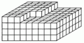
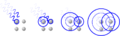
In a single H-atom an electron resides in well known orbitals. Note that the orbitals are called s,p,d in order of increasing circular current. Putting two atoms together leads to delocalized orbitals across two atoms, yielding a covalent bond. Due to the Pauli exclusion principle, every state can contain only one electron. This can be continued with more atoms. Note: This picture shows a metal, not an actual semiconductor. Continuing to add creates a crystal, which may then be cut into a tape and fused together at the ends to allow circular currents. For this regular solid the band structure can be calculated or measured. Integrating over the k axis gives the bands of a semiconductor showing a full valence band and an empty conduction band. Generally stopping at the vacuum level is undesirable, because some people want to calculate: photoemission, inverse photoemission After the band structure is determined states can be combined to generate wave packets. As this is analogous to wave packages in free space, the results are similar. An alternative description, which does not really appreciate the strong Coulomb interaction, shoots free electrons into the crystal and looks at the scattering. A third alternative description uses strongly localized unpaired electrons in chemical bonds, which looks almost like a Mott insulator.
Energy bands and electrical conduction In the classic crystalline semiconductors,electrons can have energies only within certain bands (i.e. ranges of levels of energy). Energetically, these bands are located between the energy of the ground state, the state in which electrons are tightly bound to the atomic nuclei of the material, and the free electron energy, the latter describing the energy required for an electron to escape entirely from the material. The energy bands each correspond to a large number of discrete quantum states of the electrons, and most of the states with low energy (closer to the nucleus) are full, up to a particular band called the valence band. Semiconductors and insulators are distinguished from metals because the valence band in any given metal is nearly filled with electrons under usual operating conditions, while very few (semiconductor) or virtually none (insulator) of them are available in the conduction band, the band immediately above the valence band. The ease with which electrons in the semiconductor can be excited from the valence band to the conduction band depends on the band gap between the bands. The size of this energy bandgap serves as an arbitrary dividing line (roughly 4 eV) between semiconductors and insulators. With covalent bonds, an electron moves by hopping to a neighboring bond. The Pauli exclusion principle requires the electron to be lifted into the higher anti-bonding state of that bond. For delocalized states, for example in one dimension – that is in a nanowire, for every energy there is a state with electrons flowing in one direction and another state with the electrons flowing in the other. For a net current to flow, more states for one direction than for the other direction must be occupied. For this to occur, energy is required, as in the semiconductor the next higher states lie above the band gap. Often this is stated as: full bands do not contribute to the electrical conductivity. However, as the temperature of a semiconductor rises above absolute zero, there is more energy in the semiconductor to spend on lattice vibration and on exciting electrons into the conduction band. The current-carrying electrons in the conduction band are known as "free electrons", although they are often simply called "electrons" if context allows this usage to be clear. Electrons excited to the conduction band also leave behind electron holes, i.e. unoccupied states in the valence band. Both the conduction band electrons and the valence band holes contribute to electrical conductivity. The holes themselves don't actually move, but a neighboring electron can move to fill the hole, leaving a hole at the place it has just come from, and in this way the holes appear to move, and the holes behave as if they were actual positively charged particles. One covalent bond between neighboring atoms in the solid is ten times stronger than the binding of the single electron to the atom, so freeing the electron does not imply destruction of the crystal structure. Date: 2016-01-03; view: 906
|