CATEGORIES:
BiologyChemistryConstructionCultureEcologyEconomyElectronicsFinanceGeographyHistoryInformaticsLawMathematicsMechanicsMedicineOtherPedagogyPhilosophyPhysicsPolicyPsychologySociologySportTourism
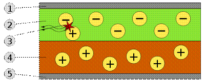
Principle of actionOLED-Display Physical organic electroluminescent display represents a solid device, consisting of a few very thin organic films made between two conductors. Submission to the conductors of a small voltage (about 2.8 volts) and causes the display to emit light. The basis of the OLED-matrix are polymers, their continual improvement largely improves the display and development of manufacturing technologies matrix. Currently, driven primarily two technologies, which showed the highest efficiency. They differ used organic materials are polymers (PLED) and macromolecule (sm-OLED). Consider them in detail we will not, because the phone's user is not critical, and very rarely in the manufacturer specifications phone with the technical nuances of manufacturing the display. Different OLED-displays decent mechanical strength, and even flexibility. However, the use of flexible substrates already liberated in a separate direction FOLED. And, finally, in contrast to the existing TFT and STN displays, OLED-displays consume significantly less power. By analogy with the other displays are also possible to use passive or active matrix. Most often, OLED-displays are used as external (or auxiliary) displays, as do the main display of the phone based on OLED-technology, at least, expensive. For the same reason, these displays are usually limited to 256 colors reproduction. For example, a display with a resolution of 94 x 94 pixels is used in LG G7030, a Samsung SGH-E700 resolution slightly smaller (96 x 64 pixels). In general, these displays look very good, providing a bright and readable picture, but, unfortunately, the sun consider anything on this display possible. Principle of action To create Organic Light Emitting Diode (OLED) are used thin-film multilayer structures consisting of layers of several polymers. When applying to the anode positive relation to the cathode voltage, the flow of electrons flowing through the device from cathode to anode. Thus the cathode gives electrons to the emission layer and the anode takes electrons from the conductive layer or in other words, the anode gives a hole in the conductive layer. Emissive layer has a negative charge and the conductive layer is positive. By electrostatic forces electrons and holes move towards each other and recombine at the meeting. This happens closer to the emissive layer, because in organic semiconductors holes have greater mobility than electrons. There is a decrease in the recombination of the electron energy, which is accompanied by the emission (emission) of electromagnetic radiation in the visible light region. Therefore the layer is called emissive. Scheme of a two-layer OLED-panel: 1. The cathode (-), 2. Emissive layer, 3. Emitted radiation, 4. Conductive layer, 5. The anode (+). The device does not work when applied to the anode, the negative relation to the cathode voltage. In this case, the holes move to the anode, and the electrons in the opposite direction to the cathode, and recombination occurs. As an anode material commonly used indium oxide doped with tin. It is transparent to visible light and has a high work function which promotes injection of holes in the polymer layer. For the manufacture of cathode often use metals such as aluminum and calcium, as they have a low work function, promotes injection of electrons into the polymer layer.
The history Andre Bernanoz (André Bernanose) and his team discovered electroluminescence in organic materials in the early 1950s by applying an alternating current high voltage to a transparent thin films of dye acridine orange and quinacrine. In 1960, researchers from The Dow Chemical Company developed the controlled alternating current electroluminescent cells using doped anthracene. The low electrical conductivity of such materials limited the development of the technology so far have not yet become available to more modern organic materials such as polyacetylene and polypyrrole. 1963 in a series of articles, scientists reported that they had observed a high conductivity in iodine-doped polypyrrole. They reached a conductivity of 1 S / cm. Unfortunately, this discovery was "lost." It was only in 1974, studied the properties of a bistable switch based on melanin with high conductivity in "on" state. This material emitted a flash of light on startup. In 1977, another group of researchers reported high conductivity in similarly oxidized and iodine-doped polyacetylene. In 2000, Alan Heeger, Alan MacDiarmid and Hideki Shirakawa were awarded the Nobel Prize in Chemistry for "the discovery and development of conductive organic polymers." References to earlier discovery was not. The first diode device was created in 1980 by Eastman Kodak. In 1990, in an article by the journal Nature scientists have reported a polymer with a green luminosity and "very high efficiency." Recently, a hybrid light-emitting layer, which uses non-conductive polymers doped with light-emitting conductive molecules. The use of the polymer provides advantages in mechanical properties without sacrificing optical properties. Light-emitting molecules have the same durability as the original polymer.
Date: 2015-12-24; view: 794
|