CATEGORIES:
BiologyChemistryConstructionCultureEcologyEconomyElectronicsFinanceGeographyHistoryInformaticsLawMathematicsMechanicsMedicineOtherPedagogyPhilosophyPhysicsPolicyPsychologySociologySportTourism
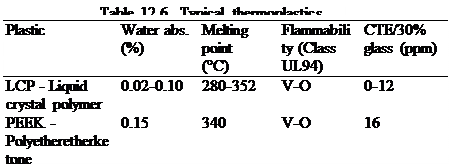
PlasticAlthough plastics were used earlier for discrete transistors, plastic packages became mainstream products with the introduction of dual-in-line packages (DIP). Such packages remained as the most common commercial products throughout the integrated circuit revolution of the late 20th century. Low manufacturing costs of such materials have them widely used by the electronics industry and other applications. However, questions regarding their use in high reliability applications have been raised. Plastic packages are permeable to water vapor and often do not consistently provide the robust seals required in high reliability applications. Products are also susceptible to cracking ("popcorning") in humid environments and during PWB soldering or rapid temperature cycling. For these reasons, plastic packages have been slow to gain wide acceptance in aerospace applications. However, some newer semiconductor designs that are only available in plastic packages are beginning to be flown in space applications. Programs such as Commercial off the Shelf (COTS), which include Plastic Encapsulated Microelectronics (PEMs), are gaining acceptance. For example, suitable PEMs were used for The Applied Physics Laboratory's Thermosphere-Ionosphere-Mesosphere Energetics and Dynamics (TIMED) program. The size, cost, and weight constraints of the TIMED mission were achieved only with commercially available devices [8].
12.2.4 Array Packaging Materials/Wafer Level Packaging Wafer Level Packaging (WLP) involves bonding of silicon structures. Such processes usually entail capping of fragile structures to ensure proper isolation from the surrounding environment. Processes vary by applications, and custom solutions are dictated by MEMS chips. Concerns for the damages that arise during assembly operations of wafer level packaging need to be addressed. Fabrication steps include dicing, pick-and-place die mounting, wire bonding, soldering, and sealing. Structural support and protection are provided by the use of a capping technique. Two approaches for encapsulation are currently in use: wafer-to-wafer bonding, and die-to-wafer bonding. The general idea of wafer-to-wafer bonding is to cap the wafer containing the MEMS structures with a separate, micromachined wafer in which a small cavity is made or a standoff ring is present. Wafer bonding uses anodic, fusion, or glass-frit sealing which is discussed in Section 12.4.2. For die-to-wafer bonding, preprocessed and diced caps are placed on the wafer by means of a flip chip bonder. With larger die, the approach offers economical advantages over wafer-to-wafer bonding; the longer bonding process time for mounting individual caps is balanced by making the wire bond pads readily accessible. This technique can be used for low-temperature sealing materials, including solder seals with her-meticity below 10–11 mbar 1/s (1 (torr/1)/s =1.31578947×10⁻⁶ (atm/cc)/s). It can also be used for thin caps [10]. 12.2.5 Custom Packaging Most packaging methods discussed in this chapter must be customized for specific applications. WLP is evolving to applications for 3D interconnect in addition to capping, shifting its application forward in the manufacturing process. Through-silicon vias are being used to connect MEMS, CMOS image sensors and memory devices. The newest requirement for wafer bonding arises from 3D integrated bonding. Two emerging packaging applications involve CMOS image sensors with backside illumination and DRAM stacking utilizing polymer adhesive bonding or direct oxide bonding. Integration of metallic bonding techniques, such as Cu diffusion, for next-generation 3D CMOS is also currently advancing rapidly. Recent packaging advances include the integration of silicon through implementation of system-in-package (SiPs) and 3D stacking of both dies and packages [11]. Date: 2015-02-28; view: 1112
|
